Deposition method of interlayer film

A deposition method and interlayer film technology, applied in the direction of coating, metal material coating process, gaseous chemical plating, etc., can solve pollution, cross-contamination and other problems, to avoid cross-contamination, improve utilization rate, and improve shipment volume effect

Inactive Publication Date: 2018-08-21
SHANGHAI HUALI INTEGRATED CIRCUTE MFG CO LTD
View PDF3 Cites 0 Cited by
  • Summary
  • Abstract
  • Description
  • Claims
  • Application Information

AI Technical Summary

Problems solved by technology

In addition, wafers enter and exit two different deposition process chambers. When a problem occurs in one of the deposition p

Method used


Image

  • Deposition method of interlayer film

Examples


Embodiment Construction

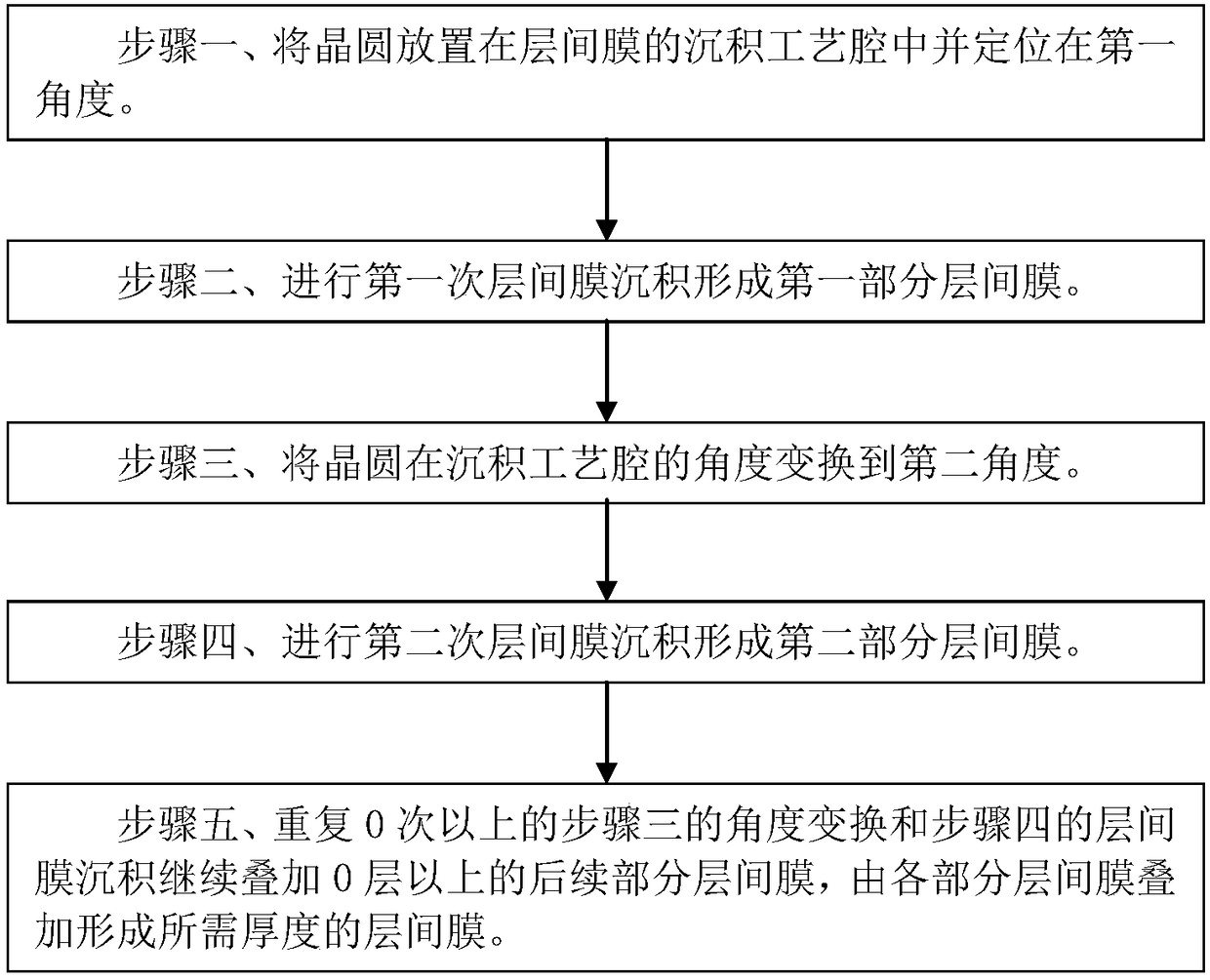
[0040] Such as figure 1 As shown, it is a flowchart of the deposition method of the interlayer film in the embodiment of the present invention. The deposition method of the interlayer film in the embodiment of the present invention includes the following steps:

[0041] Step 1, providing a wafer composed of a semiconductor substrate, placing the wafer in a chamber for depositing an interlayer film and positioning it at a first angle.

[0042] The semiconductor substrate is a silicon substrate. The material of the interlayer film is silicon oxide.

[0043] Notches for angular positioning are provided on the wafer.

[0044] In the embodiment of the present invention, the angular positioning and rotation of the wafer is realized in the deposition process chamber, and the position of the notch of the wafer is detected by an angle sensor arranged in the deposition process chamber to realize the positioning of the wafer. The angle positioning of the wafer, the wafer carrying tabl...


PUM


Abstract

The invention discloses a deposition method of an interlayer film. The deposition method of the interlayer film comprises the steps that firstly, a wafer is placed in a deposition technology cavity ofthe interlayer film and located at the first angle; secondly, interlayer film deposition is conducted for the first time, so that a first part of the interlayer film is formed; thirdly, the angle, inthe deposition technology cavity, of the wafer is changed into a second angle; fourthly, interlayer film deposition is conducted for the second time, so that a second part of the interlayer film is formed; fifthly, angle change of the third step and interlayer film deposition of the fourth step are repeatedly executed for zero time or over so that zero or over layer of follow-up parts of the interlayer film are continuously superposed, and all the parts of the interlayer film are superposed to form the interlayer film of the needed thickness. By the adoption of the deposition method of the interlayer film, the in-plane thickness evenness of the interlayer film deposited by a single deposition technology cavity can be improved, the technology is simple, cost is low, technology cavity crosscontamination can be avoided, the utilization rate of the technology cavity can be improved, the production efficiency can be improved, and the productivity can be improved.

Description

technical field [0001] The invention relates to a method for manufacturing a semiconductor integrated circuit, in particular to a method for depositing an interlayer film (ILD). Background technique [0002] The interlayer film is mainly formed before the metal layer and is used to realize the isolation between the metal layers. The metal layers are connected through contact holes or through holes passing through the interlayer film. The uniformity of the interlayer film is important for the performance of semiconductor devices. influences. In semiconductor integrated circuits, semiconductor substrates such as silicon substrates usually use wafers with a crystal structure, so the substrates in semiconductor integrated circuit manufacturing usually use wafers, and interlayer films are usually formed by chemical vapor deposition (CVD) processes. CVD Among them, plasma enhanced chemical vapor deposition (PECVD) is included. In the prior art, PECVD is mostly used for interlayer...

Claims


Application Information

Patent Timeline
IPC IPC(8): C23C16/44
CPCC23C16/44
Inventor 刘志通
Owner SHANGHAI HUALI INTEGRATED CIRCUTE MFG CO LTD
Why Eureka
Try Eureka