
Device and method for wavefront analysis

A wavefront, to-be-analyzed technology, used in measurement devices, photolithographic process exposure devices, lens position determination, etc., can solve problems such as high spatial frequency, high fringe density, interference pattern analysis, etc. The effect of high speed and fast measurement speed

Active Publication Date: 2018-08-21
CARL ZEISS SMT GMBH
View PDF8 Cites 3 Cited by
  • Summary
  • Abstract
  • Description
  • Claims
  • Application Information

AI Technical Summary

Problems solved by technology

[0006] A problem that can actually arise here is that the relevant interference pattern can no longer be resolved by the available camera-based detectors, e.g. due to too high a fringe density or too high a spatial frequency

Method used


Image

  • Device and method for wavefront analysis
  • Device and method for wavefront analysis
  • Device and method for wavefront analysis

Examples


Embodiment Construction

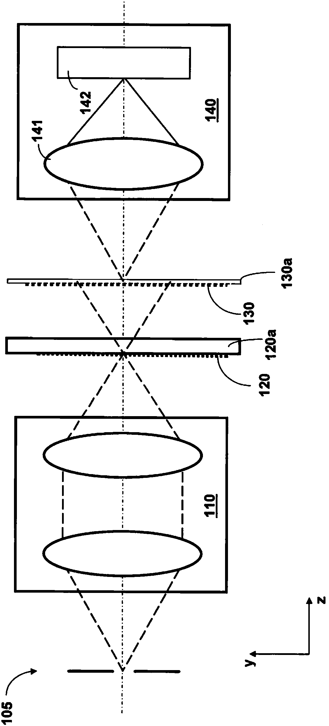
[0051] figure 1 A schematic diagram of a possible setup of a device according to the invention for wavefront detection is first shown.

[0052] exist figure 1 In , the wavefront effect marks the tested imaging optical unit as "110", which can also be any subsystem of the illumination device or the projection lens of the microlithography projection exposure device. In order to examine the wavefront effect of the imaging optical unit 110 or to analyze the wavefront of light waves passing through the imaging optical unit 110, according to figure 1 The configuration has an illumination mask 105 in the form of a perforated mask through which light from a light source (not shown) enters the imaging optical unit 110 and is incident on is the z direction) and is disposed on the first grating 120 downstream of the imaging optical unit 110 .

[0053] The first grating 120 has at least one first grating structure and is applied on a substrate designated "120a", the substrate 120a bein...


PUM


Abstract

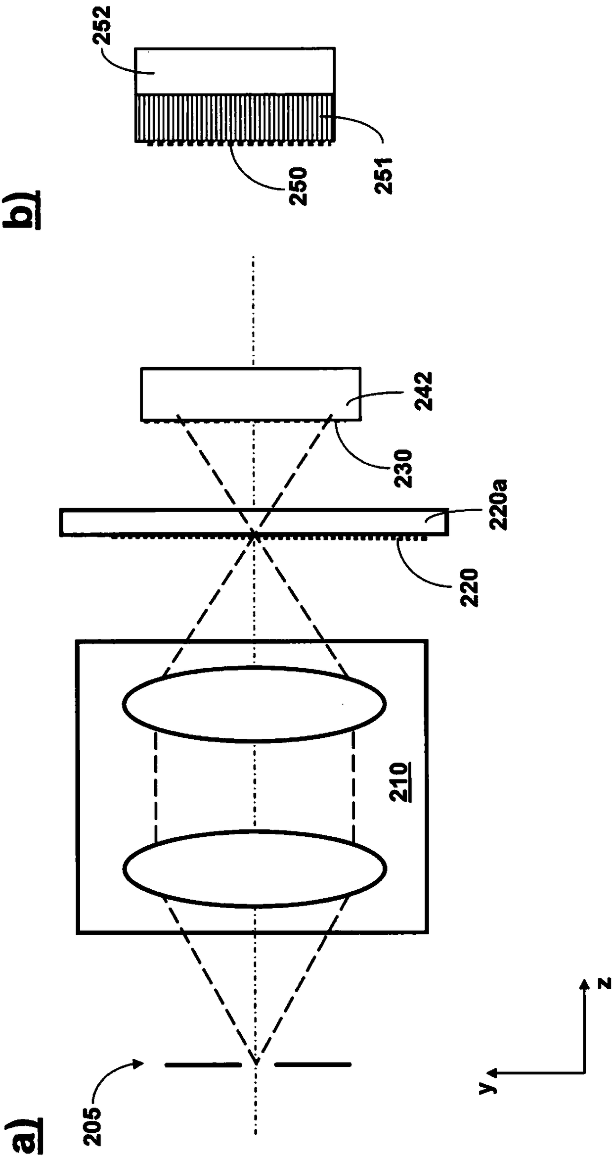
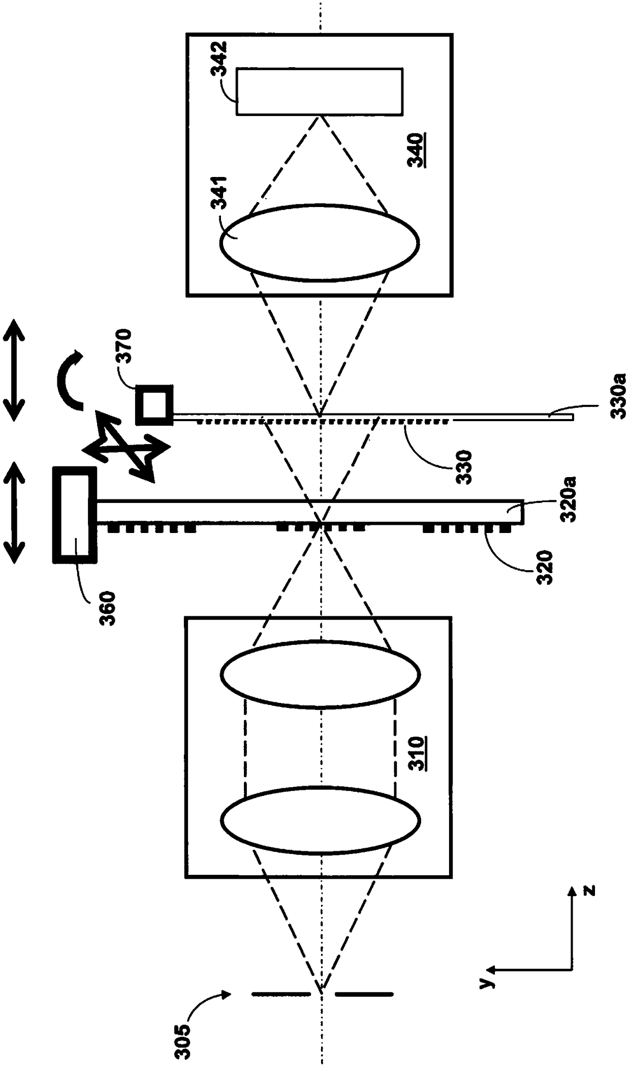
The invention relates to a device and a method for wavefront analysis. A device for wavefront analysis, which is designed for analyzing the wavefront of at least one light wave passing through an optical system, comprises at least one illumination mask (105, 205, 305, 405, 406, 407), at least one first grating (120, 220, 320, 420), which has at least one first grating structure and generates an interferogram in a predefined plane from a wavefront to be analyzed which proceeds from the illumination mask and passes through the optical system, at least one second grating (130, 230, 330, 430) arranged in said predefined plane, said at least one second grating having at least one second grating structure and generating a superimposition pattern by the superimposition of the second grating structure with the interferogram generated by the first grating, and at least one detector (140, 240, 340, 440) for detecting said superimposition pattern.

Description

[0001] Cross References to Related Applications [0002] This application claims the benefit of German patent application DE 10 2015 226 571.4 filed on December 22, 2015. The content of this application is incorporated herein by reference. technical field [0003] The present invention relates to apparatus and methods for wavefront analysis. Background technique [0004] Microlithography is used to produce microstructural components such as integrated circuits or LCDs. The microlithography process is carried out in a so-called projection exposure system with an illumination device and a projection lens. The image of the mask (reticle) illuminated by the illumination device is in this case projected by a projection lens onto a substrate (e.g. a silicon wafer) coated with a photosensitive layer (photoresist) and arranged in the image plane of the projection lens. ) to transfer the mask structure to the photosensitive coating of the substrate. [0005] Both in projection le...

Claims


Application Information

Patent Timeline
Patent Type & Authority Applications(China)
IPC IPC(8): G03F7/20G01M11/02
CPCG01M11/0271G01M11/0221G01M11/0285G03F7/706G01J9/02G01J2009/0219G03F7/70141G03F7/70266
Inventor U.韦格曼
Owner CARL ZEISS SMT GMBH
Learn More