Electron emission electrode and process for production thereof

An electron emission and electrode technology, which is applied in the direction of electrode system manufacturing, cold cathode manufacturing, discharge tube/lamp manufacturing, etc., can solve the problems of troublesome, unobtainable electron emission electrode durability, etc., achieve high emission current, optimize manufacturing and Economical effect

Inactive Publication Date: 2018-08-21
GOTTFRIED WILHELM LEIBNIZ UNIV HANNOVER
View PDF5 Cites 2 Cited by
  • Summary
  • Abstract
  • Description
  • Claims
  • Application Information

AI Technical Summary

Problems solved by technology

The known production methods are relatively complex and do not achieve the required durability of the electron-emitting electrodes, especially when used in field emission displays (FET technology)

Method used


Image

  • Electron emission electrode and process for production thereof
  • Electron emission electrode and process for production thereof
  • Electron emission electrode and process for production thereof

Examples


Embodiment Construction

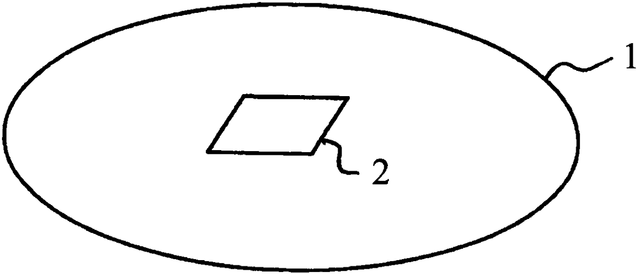
[0042] figure 1 A substrate composed of fragmented material, such as a silicon wafer, is shown. The base body 1 , which forms the electron-emitting electrode 2 , is processed according to the invention, which is explained in greater detail below with reference to partial regions of the base body 1 .

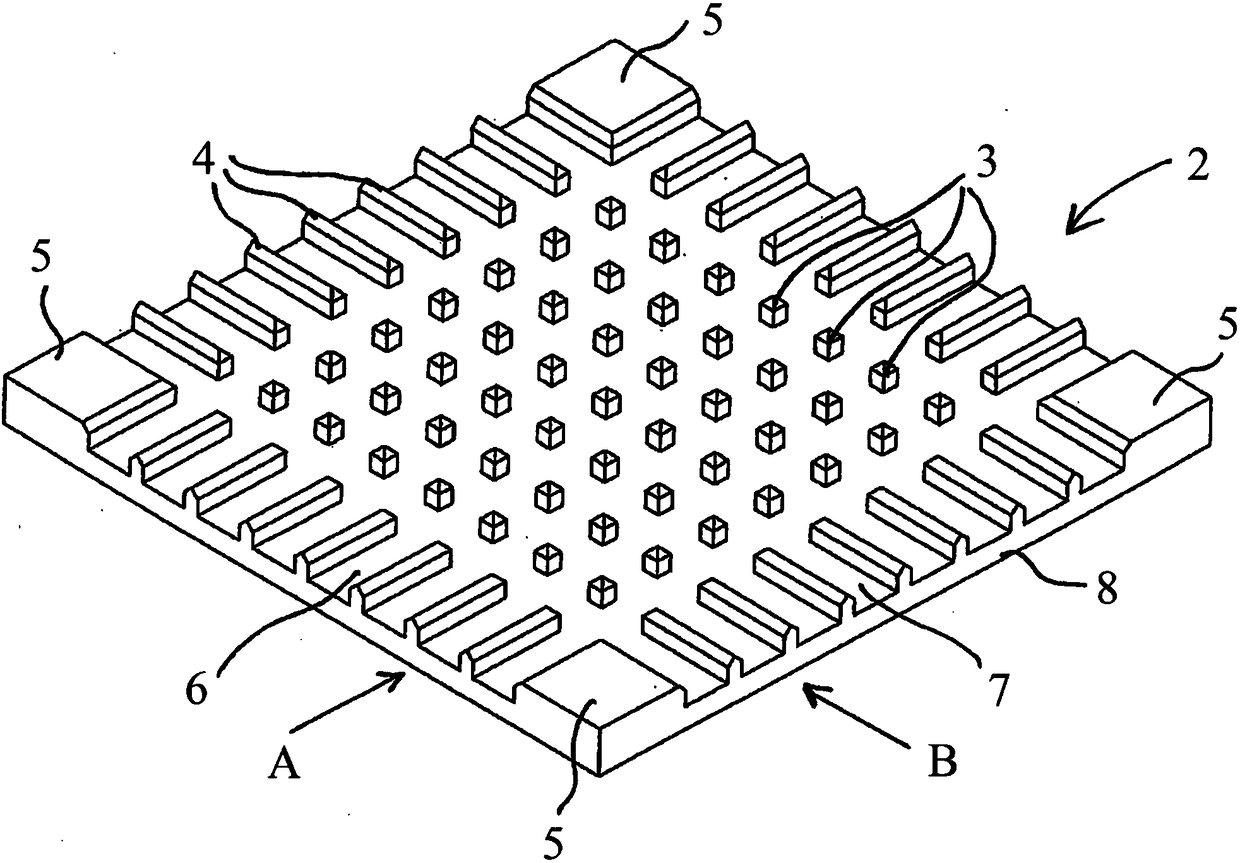
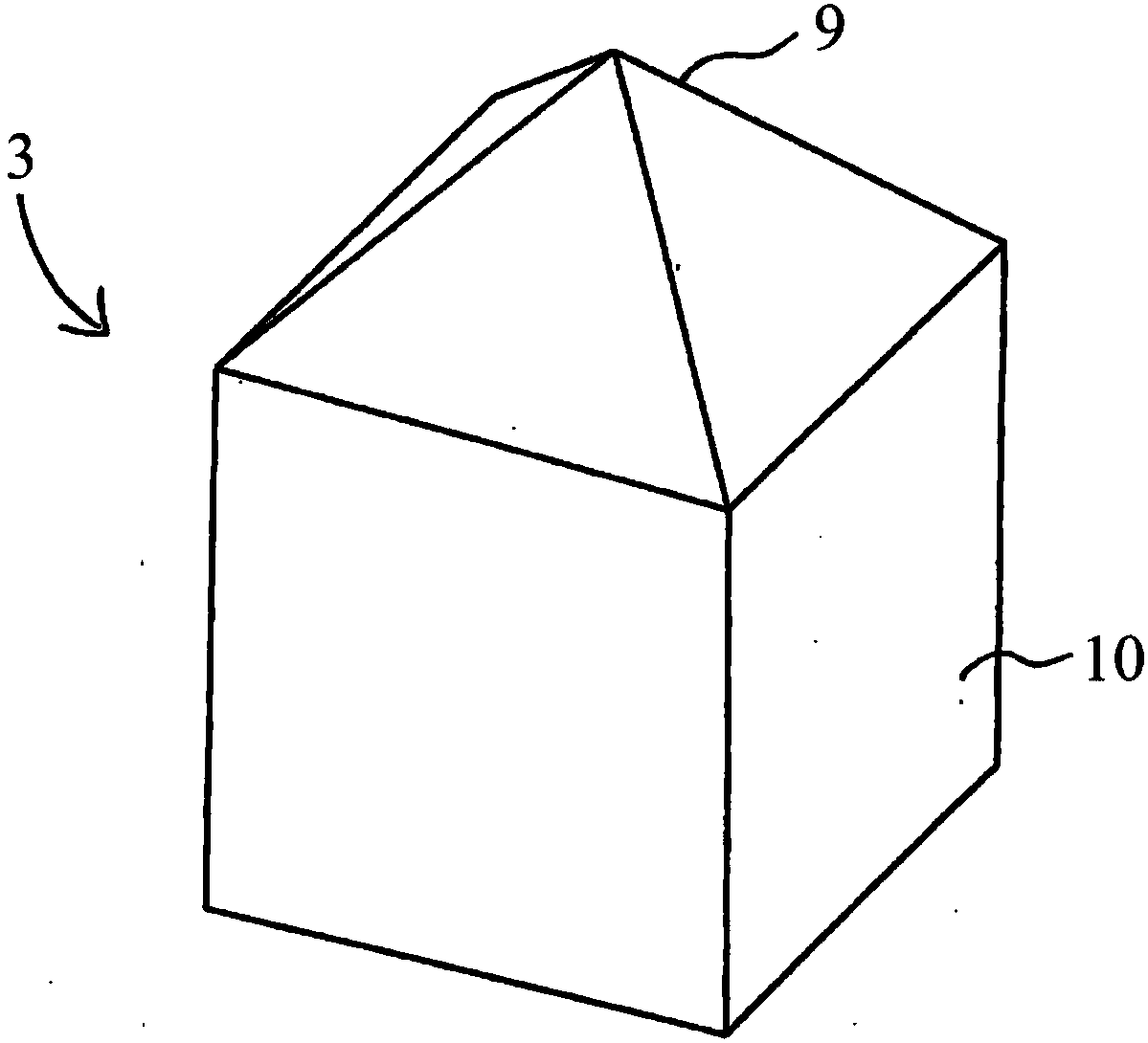
[0043] figure 2 Shown is an enlarged view of a local area in which a substrate 1 has been subjected to surface processing, by which the local area is formed as an electron emission electrode 2 having a plurality of emission tips. exist figure 2 Visible in FIG. 1 is the arrangement of a plurality of point-shaped elevations 3 which contain the emission tips of the electron emission electrodes 2 . In the edge region there are a plurality of linear elevations 4 which surround the matrix-shaped arrangement of pointed elevations 3 . In the respective end regions of the electron emission electrode 2 there is a cuboidal elevation 5 which can serve as a base region for the electron ...


PUM


Abstract

The invention relates to a process for producing an electron emission electrode (2) of an electron source, wherein the electron emission electrode has at least one emission tip (3) set up to release electrons into the environment, having the steps of a) provision of a parent body (1) made from a brittle material, b) mechanical and/or thermal surface working of the parent body to form the emissiontip, wherein brittle material is removed from the parent body at least around the emission tip. The invention also relates to an electron emission electrode of this kind and to a device having one ormore electron emission electrodes.

Description

technical field [0001] The invention relates to a method for producing an electron emission electrode of an electron source, wherein the electron emission electrode has at least one emission tip which is designed to emit electrons into the surrounding environment. Furthermore, the invention relates to such an electron-emitting electrode and to a device having one or more electron-emitting electrodes. Background technique [0002] Such electron sources with at least one electron-emitting electrode can be used in different applications, for example in electron microscopes, field emission displays or other devices. Various proposals exist for producing electron sources, for example in DE 11 2012 003 268 T5, EP 1 892 741 A1 or DE 605 15 245 T2. The known production methods are relatively complex and do not achieve the required durability of the electron emission electrodes, especially when used in field emission displays (FET technology). Contents of the invention [0003] I...

Claims


Application Information

Patent Timeline
Patent Type & Authority Applications(China)
IPC IPC(8): H01J9/02H01J1/304H01J3/02
CPCH01J1/3042H01J3/022H01J9/025
Inventor L·瑞思英A·库施M·斯图普S·齐默曼E·布内特
Owner GOTTFRIED WILHELM LEIBNIZ UNIV HANNOVER
Why Eureka
Try Eureka