

An image sensor and its manufacturing method
A technology of an image sensor and a manufacturing method, which is applied to semiconductor devices, electric solid-state devices, radiation control devices, etc., can solve the problems of increasing the multiple processing of the substrate, high cost, etc.
- Summary
- Abstract
- Description
- Claims
- Application Information
AI Technical Summary
Problems solved by technology
Method used
Image

Examples
no. 1 example
[0059] see Figure 1-9 , a method for manufacturing an image sensor, comprising the steps of:
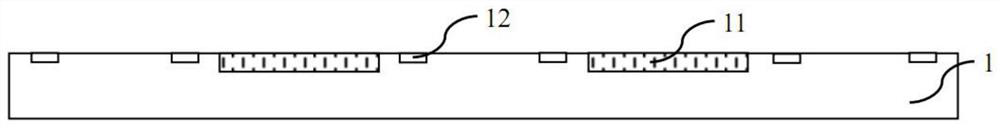
[0060] (1) A substrate 1 is provided, and the substrate 1 has an opposite first surface and a second surface, and a plurality of light receiving regions 11 are provided on the first surface and a plurality of light receiving regions 11 are provided on the first surface. Multiple electrodes 12 on both sides;
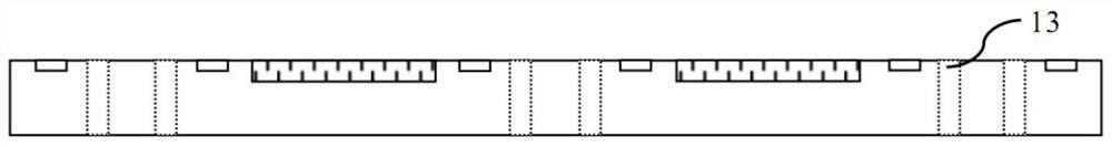
[0061] (2) forming a plurality of first through holes 13 in the substrate 1, the plurality of first through holes 13 are separated from the plurality of electrodes 12 by a certain distance;
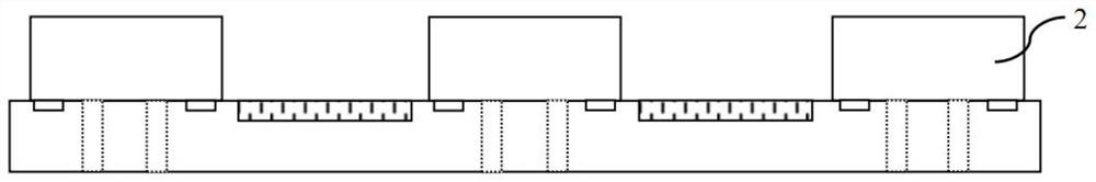
[0062] (3) Alignment marks 5 are formed near the plurality of light-receiving regions 11, and partition walls 2 formed between the plurality of light-receiving regions 11 are formed by injection molding, and the partition walls 2 cover the plurality of electrodes 12 , but does not cover the plurality of light receiving regions 11 and the alignment mark 5;
[0063] (4) A plurality of seco...
no. 2 example
[0076] see Figure 10-11 , the present invention also provides another method for manufacturing an image sensor, which is similar to the first embodiment, except that a conductive pattern connecting two light-receiving regions is added on the transparent substrate, including the following steps:
[0077] (1) A substrate is provided, the substrate has an opposite first surface and a second surface, a plurality of light receiving regions are provided on the first surface, and a plurality of light receiving regions are provided on both sides of the plurality of light receiving regions. electrodes;
[0078] (2) forming a plurality of first through holes in the substrate, the plurality of first through holes being separated from the plurality of electrodes by a certain distance;
[0079] (3) forming alignment marks near the plurality of light-receiving regions, and forming partition walls between the plurality of light-receiving regions by injection molding, the partition walls co...
no. 3 example
[0092] see Figure 12 , the present invention provides a kind of manufacturing method of image sensor again, comprises the following steps:
[0093] (1) A substrate is provided, the substrate has an opposite first surface and a second surface, a plurality of light receiving regions are provided on the first surface, and a plurality of light receiving regions are provided on both sides of the plurality of light receiving regions. electrodes;
[0094] (2) forming alignment marks near the plurality of light-receiving regions, and forming partition walls between the plurality of light-receiving regions by injection molding, the partition walls covering the plurality of electrodes but not covering the a plurality of light receiving areas and the alignment mark;
[0095] (3) forming a plurality of through holes in the partition wall, the bottom surfaces of the plurality of through holes are respectively in contact with the plurality of electrodes;
[0096] (4) forming a connector o...
PUM
 Abstract
Description
Claims
Application Information