PCB (printed circuit board) design method and PCB

A PCB board and design method technology, applied in the direction of electrical connection printed components, printed circuit components, printed circuits, etc., can solve the problems of failure to effectively improve the problem of virtual soldering, increase product costs, and prone to virtual soldering, etc., to achieve Improve the problem of virtual soldering and air bubbles, eliminate component virtual soldering, and improve product yield

Active Publication Date: 2018-08-28
GOERTEK OPTICAL TECH CO LTD
View PDF6 Cites 1 Cited by
  • Summary
  • Abstract
  • Description
  • Claims
  • Application Information

AI Technical Summary

Problems solved by technology

When factors such as stencil thickness, printing machine parameter settings, squeegee pressure, and printing speed remain unchanged, when the opening of the stencil increases by N times, the amount of solder paste 5 leaking from this opening increases by more than N times, so there is a large Due to the existence of a certain large pin in the SMT of the component 4 of the pin (the corresponding pad 3 on the multi-layer PCB board is also large if the pin is large), it will cause the large pad 3 on the corresponding multi-layer PCB board The amount of solder paste 5 is relatively more than the solder paste 5 per unit area of ​​other pads 3 of the same component, that is, the height of the solder paste 5 on the large pad 3 will be greater than the height of the solder paste 5 on the smallest pad 3. The height value is D1. When the thickness of the stencil, the parameter setting of the printing machine, the pressure of the squeegee, the printing speed and other factors are fixed, D1 will change with the size of the pad 3. Due to the existence of the height value D1, this type of package is more expensive than other packages. Packages in the form of packaging are more prone to virtual soldering
Of course, we can optimize the welding of such components 4 by changing the thickness of the stencil, the size of the opening of the stencil, the opening method, and adjusting the parameters of the printing machine. time, wasting a lot of manpower and increasing product cost

Method used


Image

  • PCB (printed circuit board) design method and PCB
  • PCB (printed circuit board) design method and PCB
  • PCB (printed circuit board) design method and PCB

Examples


Embodiment 1

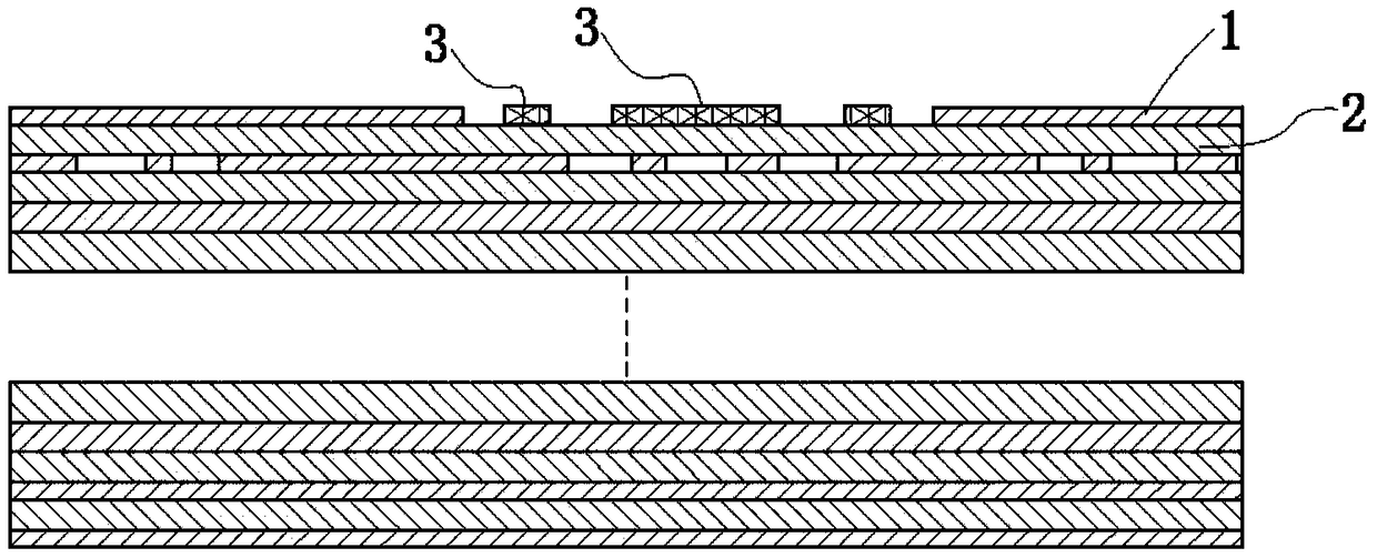
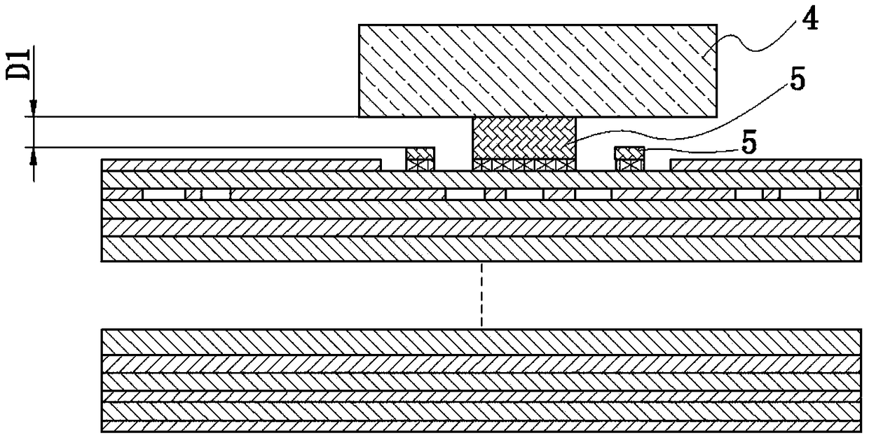
[0037] Step 1: Design the pad 3 corresponding to each pin on the multilayer PCB according to the different pins on the component 4 to be soldered;

[0038] Step 2: Set the pads 3 corresponding to the pins of different sizes on the copper layer 1 of the different traces of the PCB, and set the pads 3 corresponding to the pins with the smallest size on the surface layer. The pad 3 corresponding to the largest pin is the farthest from the surface. The vertical distance between the inner pad 3 and the PCB surface is D2. The solder paste 5 on the pad 3 is the same as the one on the surface. The thickness difference between the solder paste 5 on the pad 3 is D1, which satisfies 90% D1≤D2≤D1. In this embodiment, D1 is preferably equal to D2, and the solder paste 5 on the inner pad 3 is soldered to the surface layer. The relative height difference of the solder paste 5 on the disk 3 is zero, which more effectively ensures the elimination of the false soldering problem of the component 4;...

Embodiment 2

[0041] This embodiment is basically the same as the first embodiment, but the difference lies in:

[0042] Step 3: The copper layer 1 on the outer layer and the insulating layer 2 corresponding to the pad 3 on the inner layer are provided with openings for exposing the pad 3, and the size of the opening is smaller than the corresponding The size of the pad 3, the horizontal distance from the edge of the opening to the edge of the pad 3 is less than or equal to 2% of the corresponding side length of the pad 3.

[0043] A PCB board design method of the present invention moves the large pad 3 vertically to the inner layer of the multilayer PCB board, and D2 offsets D1, so that the height of the solder paste 5 on the large pad 3 is not too high Effectively eliminate the false soldering of component 4 caused by too much solder paste 5 on the large pad 3, improve the reliability of SMT, improve the problem of false soldering and air bubbles caused by the design of multi-layer PCB board, ...


PUM


Abstract

The invention discloses a PCB design method and a PCB, and relates to the technical field of PCB design. The PCB design method comprises the steps that bonding pads corresponding to base pins are designed on a multi-layer PCB according to different base pins on a to-be-welded element, the bonding pads corresponding to the base pins in different sizes are arranged on different wiring copper layersof the PCB, the bonding pad corresponding to the base pin in the smallest size is arranged on the surface layer, and the bonding pad corresponding to the base pin in the largest size is farthest fromthe surface layer; and opening holes used for exposing the bonding pads are formed in the positions, corresponding to the bonding pads located on the internal layer, of the wiring copper layer and aninsulation layer located on the external layer. The PCB design method and PCB can effectively eliminate element cold solder joint caused by overmuch solder paste on the large bonding pad on the multi-layer PCB, improves the reliability of SMT (surface mount technology), and improves the product yield rate.

Description

Technical field [0001] The invention belongs to the technical field of PCB board design, and particularly relates to a PCB board design method and a PCB board. Background technique [0002] Nowadays, electronic products are becoming thinner and lighter, and the upgrading speed is increasing. The functional requirements are becoming more and more abundant. The packaging of electronic devices is becoming smaller and smaller, and the packaging forms are becoming more and more abundant. The pin sizes of some packages are uneven. Some also have a larger pin. Under normal circumstances, components are mounted on a multilayer PCB board by SMT, such as figure 1 As shown, the multi-layer PCB board is a conventional design, a multi-layer PCB board with a multi-layer inner circuit board, and each layer of the circuit board includes a wiring copper layer 1 and an insulating layer 2. Such as figure 2 As shown, the pads 3 on the multilayer PCB are also designed on the surface layer (upper su...

Claims


Application Information

Patent Timeline
Patent Type & Authority Applications(China)
IPC IPC(8): H05K1/18H05K1/11
CPCH05K1/116H05K1/18
Inventor 马菲菲
Owner GOERTEK OPTICAL TECH CO LTD
Why Eureka
Try Eureka