
Pixel circuit, drive method thereof and display panel

A technology of a pixel circuit and a driving method, which is applied in the field of organic light-emitting display, achieves the effect of solving the requirements of thickness and bending, reducing the difficulty of manufacturing process, and eliminating the need for a touch panel

Inactive Publication Date: 2018-08-31
WUHAN CHINA STAR OPTOELECTRONICS SEMICON DISPLAY TECH CO LTD
View PDF7 Cites 2 Cited by
  • Summary
  • Abstract
  • Description
  • Claims
  • Application Information

AI Technical Summary

Problems solved by technology

[0005] The technical problem to be solved by the embodiments of the present invention is to provide a pixel circuit and its driving method, and a display panel, which can perfectly integrate the touch function, that is, solve the existing display panel thickness and bending requirements, and reduce the manufacturing process. Difficulty, and can also save the need to purchase touch panels

Method used


Image

  • Pixel circuit, drive method thereof and display panel
  • Pixel circuit, drive method thereof and display panel
  • Pixel circuit, drive method thereof and display panel

Examples


Embodiment Construction

[0039] In order to make the object, technical solution and advantages of the present invention clearer, the present invention will be further described in detail below in conjunction with the accompanying drawings.

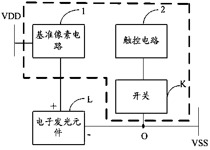
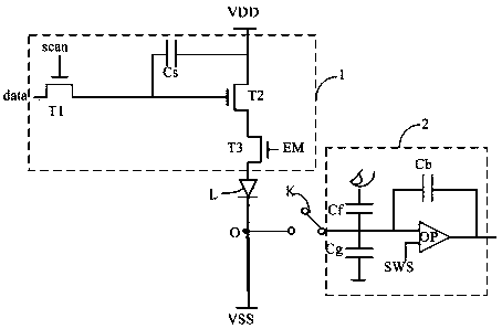
[0040] like figure 2 Shown is a pixel circuit provided in Embodiment 1 of the present invention, including a reference pixel circuit 1, a touch circuit 2, and a switch K; wherein,

[0041] One end of the reference pixel circuit 1 is connected to the DC high-voltage signal VDD, and the other end is connected to the positive electrode (+) of an electronic light-emitting element L and then connected to the DC low-voltage signal VSS through the negative electrode (-) of the electronic light-emitting element L to drive or cut off the electron. The light emitting element L emits light;

[0042] The touch circuit 2 is connected to a connection O between the negative pole (-) of the electroluminescent element L and the DC low-voltage signal VSS through the switch K, and...


PUM


Abstract

The invention provides a pixel circuit which comprises a reference pixel circuit, a touch circuit and a switch. One end of the reference pixel circuit is connected with a direct-current high-voltage signal, and the other end of the reference pixel circuit is connected with a positive electrode of an electronic light-emitting component and the is connected with a negative electrode of the electronic light-emitting component and a direct-current low-voltage signal for driving or stopping light transmission of the electronic light-emitting component; the touch circuit is connected to a certain joint between the negative electrode of the electronic light-emitting component and the direct-current low-voltage signal through a switch and used for corresponding selecting the on-off state of the switch by judging whether the reference pixel circuit drives the electronic light-emitting component to emit light or not and determining whether working is performed or not. According to the pixel circuit, the touch function can be perfectly integrated, the requirement for the thickness and bending of an existing display panel is met, the technology manufacturing difficulty is lowered, and the requirement for purchasing the touch panel can be omitted.

Description

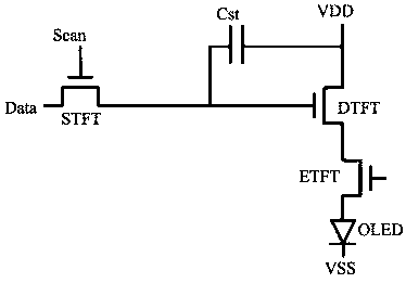
technical field [0001] The present invention relates to the technical field of organic light-emitting display, in particular to a pixel circuit, a driving method thereof, and a display panel. Background technique [0002] Compared with traditional LCD panels, AMOLED (Active Matrix / Organic Light Emitting Diode, active matrix organic light-emitting diode) panels have the characteristics of faster response, higher contrast, and wider viewing angles. Therefore, AMOLED has been favored by display technology developers. growing attention. [0003] AMOLED is driven by pixel circuits to emit light. like figure 1 As shown, the pixel circuit adopts a 3T1C design, including a switching transistor STFT, a driving transistor DTFT, a control transistor ETFT and a storage capacitor Cst. Among them, the switching transistor STFT is used to control whether the data signal enters, the driving transistor DTFT is used to control whether the driving current of the organic light-emitting diode...

Claims


Application Information

Patent Timeline
Patent Type & Authority Applications(China)
IPC IPC(8): G09G3/3225
CPCG09G3/3225
Inventor 林建宏
Owner WUHAN CHINA STAR OPTOELECTRONICS SEMICON DISPLAY TECH CO LTD
Learn More