Production technology device of semiconductor material

A production technology, semiconductor technology, applied in semiconductor/solid-state device manufacturing, electrical components, circuits, etc., can solve problems such as air pollution, unfavorable production and use of small and medium-sized enterprises, expensive cleaning equipment, etc., and achieve the effect of convenient operation and simple structure

Active Publication Date: 2018-08-31
江苏拓正茂源新能源有限公司
View PDF2 Cites 2 Cited by
  • Summary
  • Abstract
  • Description
  • Claims
  • Application Information

AI Technical Summary

Problems solved by technology

[0002] With the progress of the high-tech era, portable electronic devices such as computers and notebook computers are widely used by the public, and semiconductor manufacturing, whether it is in silicon wafers, integrated circuit manufacturing, or IC chip assembly, etc., the production and manufacturing process is quite complicated. And there are quite a lot of chemical substances used in the manufacturing process, and the residues of these chemical substances or solvents will not only pollute the air during the manufacturing process, but also affect the quality of silicon wafers, integrated circuits or IC chips. In order to improve the qualified rate of semiconductor manufacturing products, in the cleaning process of semiconductors, it is necessary to ensure that the chemical substances on the semiconductor have been cleaned, and there must be no chemical residues. Traditional cleaning equipment is expensive and occupies an area. The large area is not conducive to the production and use of small and medium-sized enterprises, and the high maintenance cost will have a huge impact on the profitability of semiconductor factories

Method used


Image

  • Production technology device of semiconductor material
  • Production technology device of semiconductor material
  • Production technology device of semiconductor material

Examples


Embodiment Construction

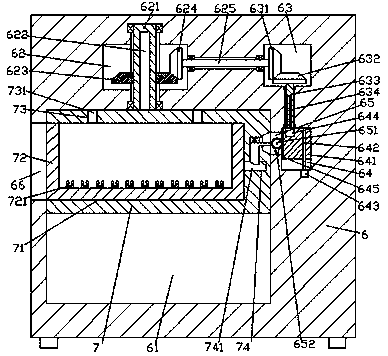
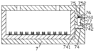
[0012] Combine below Figure 1-3 The present invention will be described in detail.

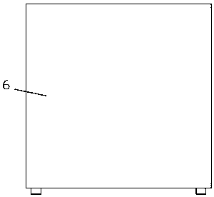
[0013] refer to Figure 1-3 According to an embodiment of the present invention, a semiconductor material production technology equipment includes a main body 6, a cleaning chamber 61 is provided in the main body 6, and a cleaning chamber 61 is provided in the left end surface of the main body 6. The opening groove 66 provided in communication, a first cavity 62 is provided in the main body 6 on the upper side of the cleaning chamber 61, and a second cavity is provided in the main body 6 on the right side of the first cavity 62. cavity 63, the main body 6 on the right side of the cleaning cavity 61 is provided with a third cavity 64, the third cavity 64 is located at the lower side of the second cavity 63, and the cleaning cavity 61 The lifting frame body 7 is connected by sliding fit, and the internal thread sleeve 621 extending up and down is connected with the rotation fit in the first c...


PUM


Abstract

The invention discloses a production technology device of a semiconductor material. The device is composed of a main machine body; and a cleaning cavity is formed inside the main machine body. An opening slot communicated with the cleaning cavity is formed in the end surface of the left side of the main machine body. A first cavity is arranged in the main machine body at the upper side of the cleaning cavity; a second cavity is arranged in the main machine body at the right side of the first cavity; a third cavity is arranged in the main machine body at the right side of the cleaning cavity; and the third cavity is arranged at the lower side of the second cavity. In addition, a lifting rack is connected inside the cleaning cavity in a sliding fit manner; an inner threaded bush extending upand down is connected in the first cavity in a normal running fit manner; the tail end of the bottom of the inner threaded bush is communicated with the top of the cleaning cavity; a lifting screw rod extending downwardly is connected in the inner threaded bush in a screw-thread fit manner; and the extended tail of the bottom of the lifting screw rod is connected with the end surface of the top of the lifting rack in a stationary fit manner.

Description

technical field [0001] The invention relates to the technical field of semiconductor cleaning and processing, in particular to a semiconductor material production technical equipment. Background technique [0002] With the progress of the high-tech era, portable electronic devices such as computers and notebook computers are widely used by the public, and semiconductor manufacturing, whether it is in silicon wafers, integrated circuit manufacturing, or IC chip assembly, etc., the production and manufacturing process is quite complicated. And there are quite a lot of chemical substances used in the manufacturing process, and the residues of these chemical substances or solvents will not only pollute the air during the manufacturing process, but also affect the quality of silicon wafers, integrated circuits or IC chips. In order to improve the qualified rate of semiconductor manufacturing products, in the cleaning process of semiconductors, it is necessary to ensure that the c...

Claims


Application Information

Patent Timeline
Patent Type & Authority Applications(China)
IPC IPC(8): H01L21/67
CPCH01L21/67023H01L21/67207H01L21/67253
Inventor 何冠阅
Owner 江苏拓正茂源新能源有限公司
Why Eureka
Try Eureka