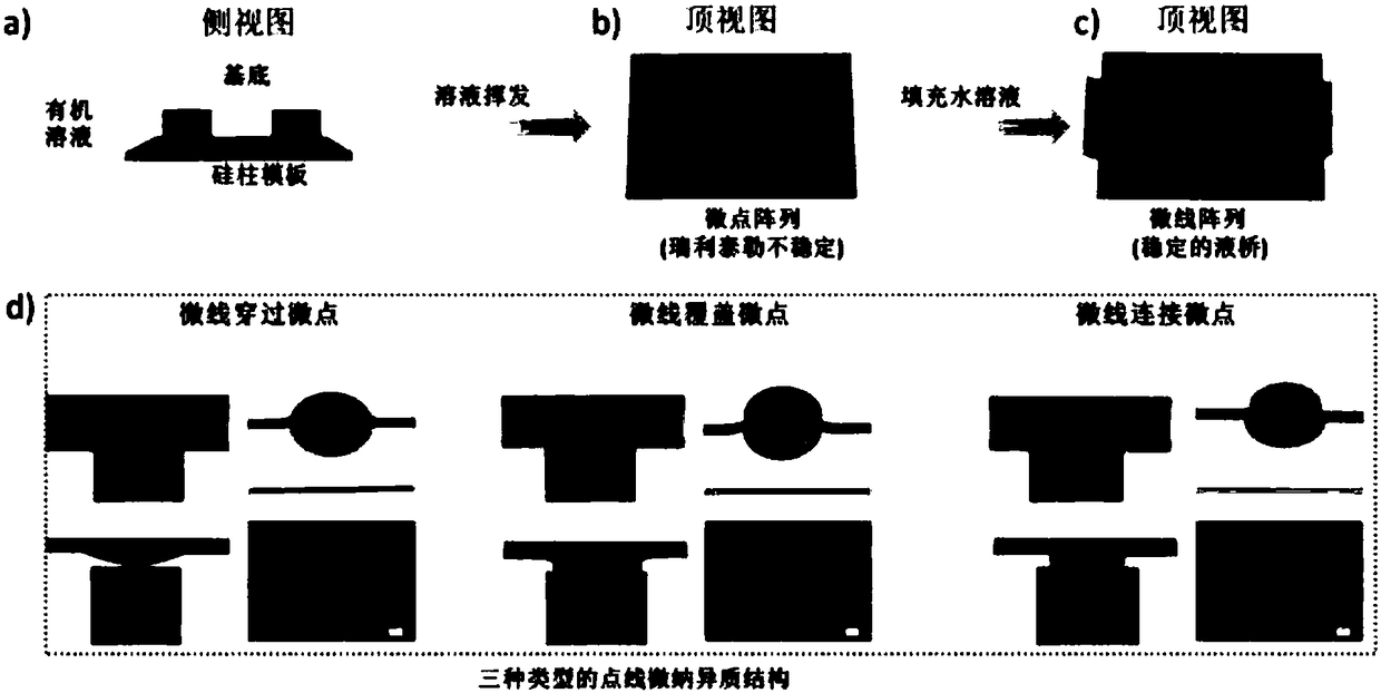
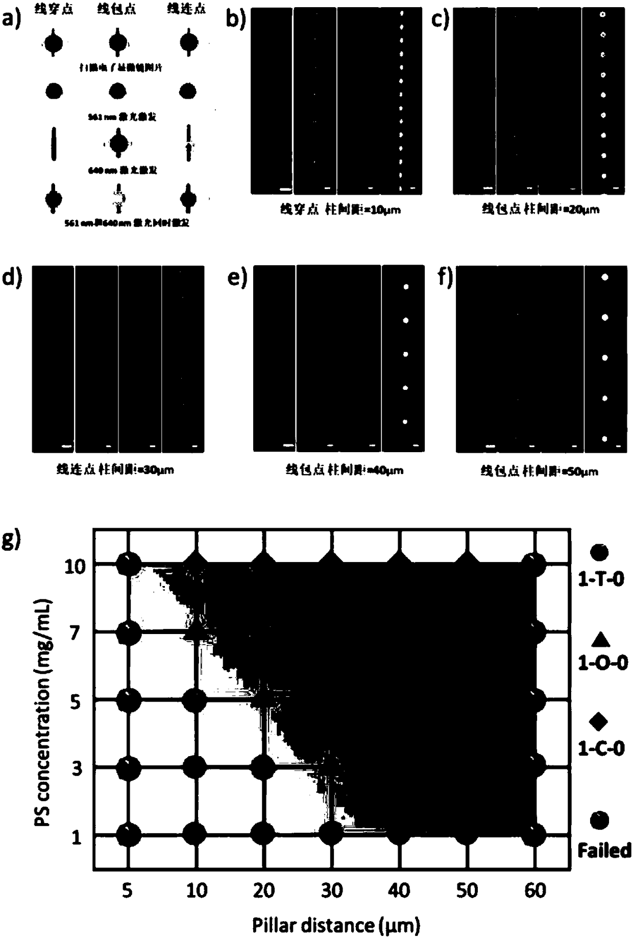
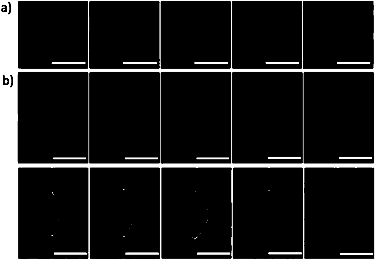
Printing method of functional micro nano heterostructure
A printing method and heterostructure technology, which is applied in the printing field of functional micro-nano heterostructures, can solve the problems of chaotic connection methods of heterogeneous structures, difficulty in controlling solutions, etc., and achieve the effect of precise and controllable interface morphology
- Summary
- Abstract
- Description
- Claims
- Application Information
AI Technical Summary
Problems solved by technology
Method used
Image

Examples
Embodiment 1
[0039] The mass content of CdS prepared by CdS quantum dots with a particle size of 5nm, polystyrene and o-dichlorobenzene is 0.2%, the mass content of polystyrene is 0.1%, and the balance is o-dichlorobenzene. Take 10 microliters from the liquid gun and spread it evenly on the photolithographic circular silicon column template; cover the silicon substrate on the silicon column template covered with the assembly solution, and let the solvent evaporate evenly at 80°C; take out the device and let it cool at room temperature, and again Inject 10 microliters of the assembly solution prepared by CdS quantum dots with a particle size of 5nm, polyvinyl alcohol, sodium lauryl sulfate and water, wherein the mass content of CdS is 0.2%, and the mass content of polyvinyl alcohol is 0.5%. The mass content of sodium alkyl sulfate is 0.2%, and the balance is water, so that the solvent is uniformly volatilized at 50° C., and after the water in the assembly solution volatilizes, a silicon wafe...
Embodiment 2
[0041] The mass content of CdS prepared by CdS quantum dots with a particle size of 5nm, polystyrene and o-dichlorobenzene is 0.2%, the mass content of polystyrene is 0.5%, and the balance is o-dichlorobenzene. Take 10 microliters from the liquid gun and spread it evenly on the photolithographic circular silicon column template; cover the silicon substrate on the silicon column template covered with the assembly solution, and let the solvent evaporate evenly at 80°C; take out the device and let it cool at room temperature, and again Inject 10 microliters of the assembly solution prepared by CdS quantum dots with a particle size of 5nm, polyvinyl alcohol, sodium lauryl sulfate and water, wherein the mass content of CdS is 0.2%, and the mass content of polyvinyl alcohol is 0.5%. The mass content of sodium alkyl sulfate is 0.2%, and the balance is water, so that the solvent is uniformly volatilized at 50° C., and after the water in the assembly solution volatilizes, the silicon ch...
Embodiment 3
[0043] The mass content of CdS prepared by CdS quantum dots with a particle size of 5nm, polystyrene and o-dichlorobenzene is 0.2%, the mass content of polystyrene is 1%, and the balance is o-dichlorobenzene. Take 10 microliters from the liquid gun and spread it evenly on the photolithographic circular silicon column template; cover the silicon substrate on the silicon column template covered with the assembly solution, and let the solvent evaporate evenly at 80°C; take out the device and let it cool at room temperature, and again Inject 10 microliters of the assembly solution prepared by CdS quantum dots with a particle size of 5nm, polyvinyl alcohol, sodium lauryl sulfate and water, wherein the mass content of CdS is 0.2%, and the mass content of polyvinyl alcohol is 0.5%. The mass content of sodium alkyl sulfate is 0.2%, and the balance is water, so that the solvent is uniformly volatilized at 50°C, and after the water in the assembly solution is volatilized, a micro-nano st...
PUM
| Property | Measurement | Unit |
|---|---|---|
| Particle size | aaaaa | aaaaa |
| Particle size | aaaaa | aaaaa |
| Particle size | aaaaa | aaaaa |
Abstract
Description
Claims
Application Information
PatSnap Eureka turns technology decisions into work you can execute. Powered by our Innovation Knowledge Graph, it runs expert workflows across engineering, life sciences, materials and intellectual property. Get your review-ready output in minutes.


