Normally-closed gallium nitride HEMT device

A gallium nitride, normally closed technology, applied in the direction of semiconductor devices, electrical components, circuits, etc., can solve the problem of low output current intensity, achieve the effect of increasing output current, enhancing density, and suppressing the effect of current collapse

Pending Publication Date: 2018-09-04
JIANGSU CORENERGY SEMICON CO LTD
View PDF0 Cites 4 Cited by
  • Summary
  • Abstract
  • Description
  • Claims
  • Application Information

AI Technical Summary

Problems solved by technology

This will cause the output current intensity of this normally closed HEMT device to be small, which is smaller than that of the normally open device
[0004] There are at least the following problems in the prior art: the output current intensity of the normally closed GaN HEMT device is small, which is smaller than that of the normally open device

Method used


Image

  • Normally-closed gallium nitride HEMT device

Examples


Embodiment Construction

[0024] An embodiment of the present application provides a normally-off gallium nitride HEMT device.

[0025] In order to enable those skilled in the art to better understand the technical solutions in the present application, the technical solutions in the embodiments of the present application will be clearly and completely described below in conjunction with the drawings in the embodiments of the present application. Obviously, the described The embodiments are only some of the embodiments of the present application, but not all of them. Based on the embodiments in this application, all other embodiments obtained by persons of ordinary skill in the art without creative efforts shall fall within the scope of protection of this application.

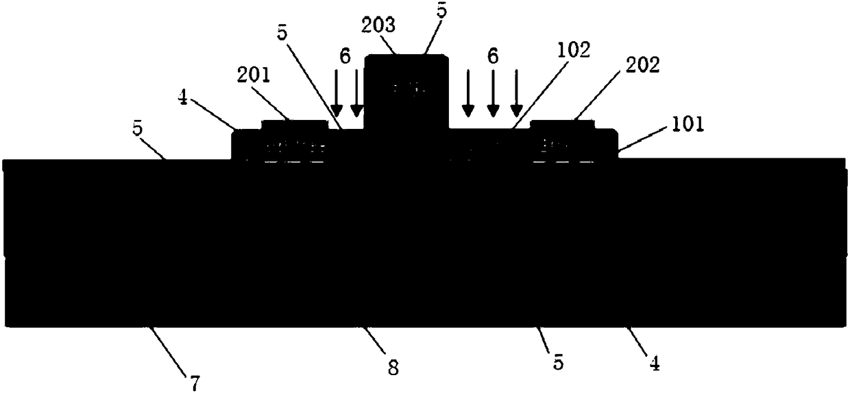
[0026] figure 1 It is a structural schematic diagram of an embodiment of a normally-off gallium nitride HEMT device described in this application. Although the present application provides device structures as shown in the following em...


PUM


Abstract

The invention provides a normally-closed gallium nitride HEMT device. The device comprises a heterostructure as well as a source electrode, a drain electrode and grid electrode which are connected with the heterostructure, wherein the heterostructure comprises a first semiconductor layer as a channel layer; a second semiconductor layer as a barrier layer is formed on the first semiconductor layer;a p-type semiconductor layer is formed between the second semiconductor layer and the grid electrode, two-dimensional electron gas is produced between the first semiconductor layer and the second semiconductor layer and disappears right below the p-type semiconductor layer; and a dielectric layer as a passivation layer is settled on the upper surface of the heterostructure, and pre-selected metalions are injected into the dielectric layer right above a region in which the two-dimensional electron gas usually exits. By virtue of each embodiment provided by the invention, the density of the two-dimensional electron of the normally-closed HEMT device can be effectively increased.

Description

technical field [0001] The present application relates to the technical field of semiconductor devices, in particular to a normally-off gallium nitride HEMT device. Background technique [0002] Due to the existence of two-dimensional electron gas between the channel layer and the barrier layer of GaN HEMT (High Electron Mobility Transistor, high electron mobility transistor), GaN HEMT is a normally-on device. [0003] In order to realize the normally closed property of the gallium nitride HEMT device, that is, it is only turned on when there is a forward bias voltage on the gate. In the prior art, a layer of p-type semiconductor is usually placed on the top of the barrier layer, but in order to achieve a reasonable forward gate bias, it is necessary to reduce the thickness of the barrier layer or the content of Al to realize the initial two-dimensional electron gas balance. This will cause the output current intensity of the normally closed HEMT device to be smaller tha...

Claims


Application Information

Patent Timeline
Patent Type & Authority Applications(China)
IPC IPC(8): H01L29/778H01L29/06
CPCH01L29/778H01L29/0603H01L29/0684
Inventor 李亦衡张葶葶朱廷刚夏远洋
Owner JIANGSU CORENERGY SEMICON CO LTD
Why Eureka
Try Eureka