
Deep drain region-equipped lateral double-diffused metal oxide composite semiconductor field effect transistor and manufacturing method thereof

A technology of lateral double-diffusion and composite semiconductors, which is applied in semiconductor/solid-state device manufacturing, semiconductor devices, electrical components, etc., can solve the problems of device withstand voltage drop, breakdown, etc., to improve vertical withstand voltage, improve breakdown voltage, Improve the effect of limit relationship

Active Publication Date: 2018-09-07
XIDIAN UNIV
View PDF6 Cites 5 Cited by
  • Summary
  • Abstract
  • Description
  • Claims
  • Application Information

AI Technical Summary

Problems solved by technology

[0003] In order to further improve the withstand voltage capability of LDMOS, methods such as RESURF technology and adding field plates can be used to optimize the peak electric field distribution on the surface; however, there are still hig

Method used


Image

  • Deep drain region-equipped lateral double-diffused metal oxide composite semiconductor field effect transistor and manufacturing method thereof

Examples


Embodiment Construction

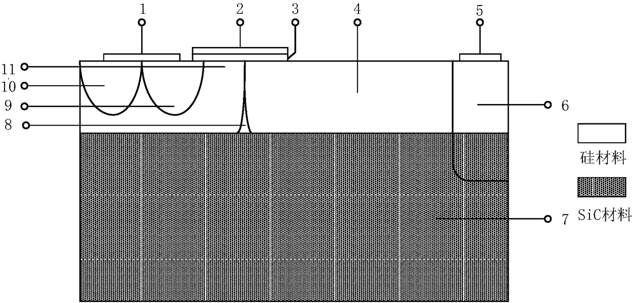
[0043] Such as figure 1 As shown, the lateral double-diffused metal oxide compound semiconductor field effect transistor with deep drain region of the present invention includes:

[0044] a substrate 7 of silicon carbide material,

[0045] A silicon epitaxial layer 8 formed by growing or bonding on the substrate 7;

[0046] A base region 11 and a drift region 4 formed by ion implantation or thermal diffusion based on the silicon epitaxial layer 8;

[0047] An active region formed by a field oxygen oxidation process on the base region 11 and the drift region 4;

[0048] A gate insulating layer 3 and a gate electrode 2 grown on the active region;

[0049] The source region 9 and the channel formed by ion implantation on the side of the base region 11 adjacent to the drift region 4;

[0050] The drain region 6 formed by ion implantation on the side of the drift region 4 away from the gate electrode 2;

[0051] A channel substrate contact 10 formed by ion implantation outside...


PUM


Abstract

The invention provides a deep drain region-equipped lateral double-diffused metal oxide composite semiconductor field effect transistor (LDMOS) and a manufacturing method thereof. According to the LDMOS device, a silicon carbide material is combined with a silicon material, and a silicon epitaxial layer is formed on a silicon carbide substrate through a heteroepitaxy technology or a bonding technology; and by adopting a deep drain region structure, the lower end of the drain region can deep into the silicon carbide substrate. Silicon carbide is a wide band-gap semiconductor and has relativelyhigh critical breakdown electric field, so that the deep drain region structure can introduce the high electric field peak value in the drain region to silicon carbide, thereby optimizing the longitudinal electric field distribution of the device, finally enabling breakdown to occur close to the drain region silicon/silicon carbide interface; therefore, the breakdown voltage of the device is improved, and the extreme relation between the breakdown voltage and the specific on-resistance in the body silicon LDMOS device can be improved; and in addition, compared with the silicon material, the silicon carbide material is relatively high in heat conductivity, and by taking the silicon carbide material as the substrate, heat dissipation of the device can be facilitated, so that the silicon carbide material can be used for manufacturing a power device which works in a high temperature condition.

Description

technical field [0001] The invention relates to the field of power semiconductor devices, in particular to a lateral double-diffusion metal oxide composite semiconductor field effect transistor. Background technique [0002] As the core of power electronics technology, the breakthrough and innovation of power semiconductor devices lead the development of this field. Among them, the lateral double diffusion MOSFET (LDMOS) uses double diffusion technology to form a conductive channel, which increases the driving current and improves the withstand voltage. It has the advantages of easy driving, easy integration, high withstand voltage, high switching speed, high input impedance, etc., making it widely used in various fields. [0003] In order to further improve the withstand voltage capability of LDMOS, methods such as RESURF technology and adding field plates can be used to optimize the peak electric field distribution on the surface; however, there are still high electric fie...

Claims


Application Information

Patent Timeline
IPC IPC(8): H01L29/78H01L29/06H01L29/267H01L21/336
CPCH01L29/0615H01L29/267H01L29/66068H01L29/7816
Inventor 段宝兴黄芸佳王彦东杨鑫孙李诚杨银堂
Owner XIDIAN UNIV
Learn More