Combined mask plate, semiconductor device, and forming method of same

A mask and mask layer technology used in the field of semiconductors

Pending Publication Date: 2018-09-11
CHANGXIN MEMORY TECH INC
View PDF5 Cites 7 Cited by
  • Summary
  • Abstract
  • Description
  • Claims
  • Application Information

AI Technical Summary

Problems solved by technology

[0006] The purpose of the present invention is to provide a combination mask to solve the problem that the existing combination mask easily defines undesired grids

Method used


Image

  • Combined mask plate, semiconductor device, and forming method of same
  • Combined mask plate, semiconductor device, and forming method of same
  • Combined mask plate, semiconductor device, and forming method of same

Examples


Embodiment 1

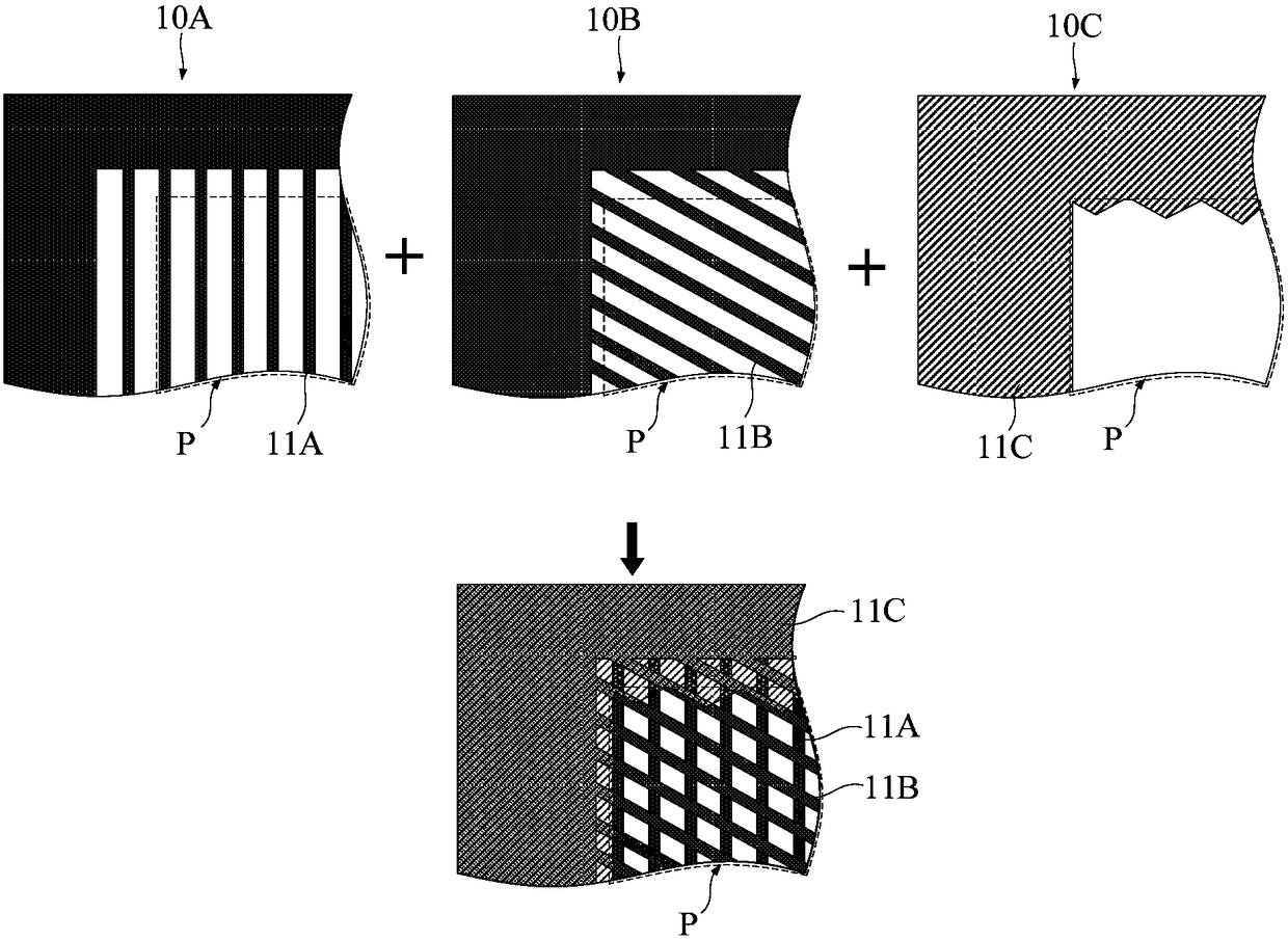
[0087] Figure 3a It is a schematic structural diagram of the combined mask plate in the first implementation of the present invention, Figure 3b for Figure 3a The mask pattern of the combined mask in Embodiment 1 of the present invention, where the first mask and the second mask are superimposed on each other, Figure 3c for Figure 3a Shown is the mask pattern of the combined mask in Embodiment 1 of the present invention after the three masks are superimposed on each other. combine Figure 3a ~ Figure 3c As shown, the combined mask includes:

[0088] The first mask plate 100A is formed with a plurality of parallel first lines 110A extending along the first direction (Y direction), and the first lines completely correspond to the array region P;

[0089] The second mask plate 100B is formed with a plurality of parallel second lines 110B extending along the second direction (Z direction), and the second lines 110B correspondingly pass through the array area P and extend...

Embodiment 2

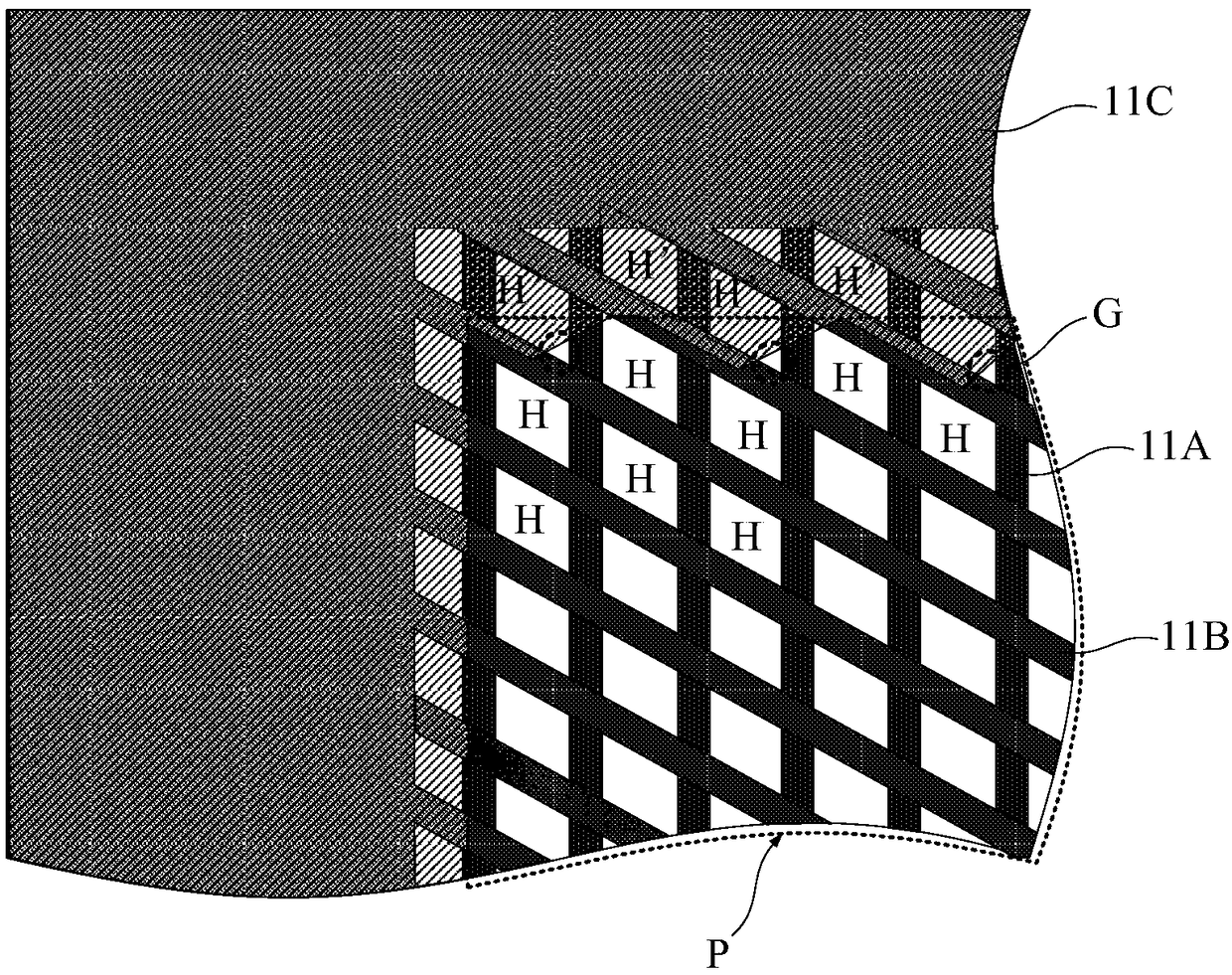
[0118] The difference from Embodiment 1 is that in this embodiment, the extension direction of the first line of the first mask is not parallel to the straight edge of the first exposed area of ​​the third mask, nor is it parallel to the straight edge of the third mask. The straight edge of the second exposed area of ​​the second mask; the second line of the same second mask is not parallel to the straight edge of the first exposed area of ​​the third mask, nor parallel to the straight edge of the second exposed area of ​​the third mask side. In this way, in the inner array defined by the first lines and the second lines, all the boundaries are non-linear boundaries (for example, wavy boundaries).

[0119] Figure 4a It is a schematic structural diagram of the combined mask plate in the second implementation of the present invention, Figure 4b for Figure 4a The mask pattern of the composite mask in the second embodiment of the present invention after the first mask and th...

Embodiment 3

[0125] Based on the above combined mask, the present invention also provides a method for forming a semiconductor device. Figure 5 It is a schematic flowchart of a method for forming a semiconductor device in Embodiment 3 of the present invention. Such as Figure 5 As shown, in this embodiment, the method for forming the semiconductor device includes:

[0126] Step S100, providing a substrate on which a mask layer is formed;

[0127] Step S200, performing a photolithography process using the combined mask as described above to form an array of openings in the mask layer, and the pattern of the array of openings is defined by the overlapping of the combined mask;

[0128] Step S300 , using the mask layer formed with the array of openings as a mask to etch the substrate, so as to form an array of through holes corresponding to the array of openings in the array region of the substrate.

[0129] Since the combined mask as described above can be used to define the grid corresp...


PUM

PropertyMeasurementUnit
hardnessaaaaaaaaaa

Abstract

The invention provides a combined mask plate, a semiconductor device, and a forming method of same. First lines on a first mask plate and second lines on a second mask plate define an enclosed array,which is located in an area range of an array zone defined by a mask pattern on a third mask plate; then by means of the mask pattern on a third mask plate and the second line which extends from the enclosed array, edge division is further defined; in such way, the edge division is accurately defined without extra definition of unexpected division. When the combined mask plate is used for formingthe semiconductor device, correspondingly, a through-hole array can be accurately prepared without extra preparation of holes in unexpected shapes.

Description

technical field [0001] The invention relates to the technical field of semiconductors, in particular to a combined mask, a semiconductor device and a forming method thereof. Background technique [0002] With the continuous advancement of semiconductor technology, the process nodes of semiconductor devices are constantly decreasing, which correspondingly makes the window of the photolithography process smaller and smaller. Based on this, a double-patterning lithography technique was proposed. For example, a denser and smaller hole (Hole) array can be prepared by using double-patterning lithography technology. [0003] Specifically, in the photolithography process used to define the hole array, it is usually necessary to use two masks, and two kinds of lines extending in different directions are respectively formed on the two masks, so that when the two masks When the plates are superimposed to define the hole array, the two lines on the two mask plates intersect to define ...

Claims


Application Information

Patent Timeline
Patent Type & Authority Applications(China)
IPC IPC(8): G03F1/68G03F1/62
CPCG03F1/62G03F1/68
Inventor 吴晗
Owner CHANGXIN MEMORY TECH INC
Why Eureka
Try Eureka