Overvoltage protection self-recovery energy-saving LED drive power source
A LED drive and overvoltage protection technology, applied in the direction of electric light source, electroluminescent light source, light source, etc., can solve the problems of reducing maintenance costs, LED drive power cannot be self-recovery, etc., to reduce maintenance costs, reduce costs and volume , the effect of simple peripheral circuit
- Summary
- Abstract
- Description
- Claims
- Application Information
AI Technical Summary
Problems solved by technology
Method used
Image

Examples
specific Embodiment 1
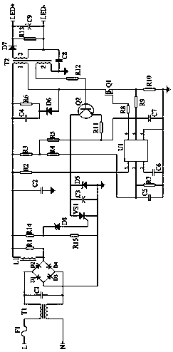
[0032] see figure 1 As shown, the present invention is an overvoltage protection self-recovery energy-saving LED drive power supply, including: mains input circuit, rectifier bridge, overvoltage protection circuit, drive chip U1, NPN transistor Q2, power switch tube Q1, switching transformer T2 and power output;
[0033] The mains input circuit is sequentially connected to the drive chip U1 through the rectifier bridge and the overvoltage protection circuit; the drive chip U1 is connected to the power output terminal through the power switch tube Q1 and the switching transformer T2 in turn; the drive chip U1 controls the load output of the power output terminal; among them, The drive chip U1 is connected to the switching transformer T2 through the NPN transistor Q2; one side of the switching transformer T2 is provided with a coil 1 and a coil 2, and the other side of the switching transformer T2 is provided with a coil 3; among them, the coil 1 is connected in parallel with a...
specific Embodiment 2
[0041] In this embodiment, the working process of the driver chip U1 is as follows, including two working states:
[0042] When the power switch tube Q1 is turned on: the driver chip U1 starts to work, and the drive signal is output from pin 6 to the gate of the power switch tube Q1. After the power switch tube Q1 is turned on, it stores energy for the switching transformer T2. What is the current signal sent by R10, when the current signal voltage is greater than the output voltage of the internal multiplier of the drive chip U1, pin 6 stops outputting the drive signal and turns off the power switch tube Q1;
[0043] When the power switch tube Q1 is turned off: after the power switch tube Q1 is turned off, the switching transformer T2 starts to discharge the load, and the pin 5 of the driver chip U1 detects the zero current detection signal sent by the NPN transistor Q2. When the zero current detection signal voltage When it drops to 0.35V, pin 6 of the driver chip U1 starts ...
specific Embodiment 3
[0045] In this embodiment, the working process of the overvoltage protection circuit is as follows:
[0046] The overvoltage protection self-recovery circuit is composed of resistors R14, R15, voltage regulator tube D8 and one-way thyristor VS1;
[0047] When the input mains voltage is normal, the DC voltage after the rectifier bridge, the voltage obtained by dividing the resistor R14 and the resistor R15, is not enough to make the voltage regulator D8 conduct in reverse, and the voltage regulator D8 is in a disconnected state. The thyristor VS1 is also disconnected, which has no effect on the work of the driver chip U1.
[0048] When the input mains voltage is too high and reaches 280V, the voltage obtained by dividing the voltage by resistor R14 and resistor R15 will cause the voltage regulator tube D8 to conduct in reverse, and the voltage regulator tube D8 will short-circuit the 1 pin of the driver chip U1 after reverse conduction. Pin power supply, U1 loses the power sup...
PUM
 Abstract
Description
Claims
Application Information
 - R&D
- Intellectual Property
- Life Sciences
- Materials
- Tech Scout
- Unparalleled Data Quality
- Higher Quality Content
- 60% Fewer Hallucinations
Browse by: Latest US Patents, China's latest patents, Technical Efficacy Thesaurus, Application Domain, Technology Topic, Popular Technical Reports.
© 2025 PatSnap. All rights reserved.Legal|Privacy policy|Modern Slavery Act Transparency Statement|Sitemap|About US| Contact US: help@patsnap.com