Material receiving device suitable for silicon wafer production line

A material receiving device and production line technology, applied in transportation and packaging, electrical components, semiconductor/solid-state device manufacturing, etc., can solve the problems of bad product mixing, high labor intensity, high labor cost, reduce labor costs, and reduce secondary damage, simple effect

Pending Publication Date: 2018-09-14
FOLUNGWIN AUTOMATIC EQUIP CO LTD
View PDF0 Cites 1 Cited by
  • Summary
  • Abstract
  • Description
  • Claims
  • Application Information

AI Technical Summary

Problems solved by technology

The traditional method is manual collection, which has high labor costs, high labor intensity, and low efficiency; and the splint is usually used to align the silicon wafer during the receiving process, which will inevitably cause se

Method used


Image

  • Material receiving device suitable for silicon wafer production line
  • Material receiving device suitable for silicon wafer production line
  • Material receiving device suitable for silicon wafer production line

Examples


Example Embodiment

[0018] The idea, specific structure and technical effects of the present invention will be further described below in conjunction with the accompanying drawings, so as to fully understand the purpose, features and effects of the present invention.

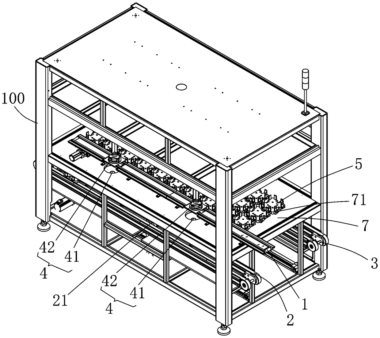
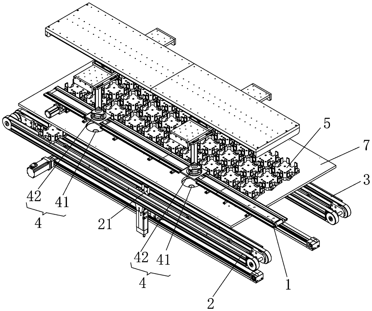
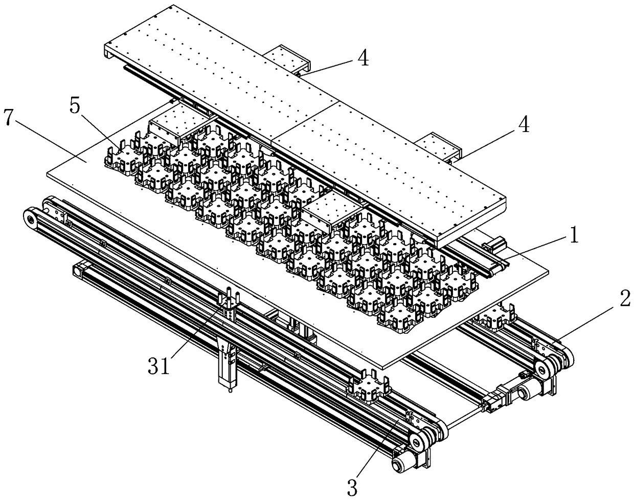
[0019] refer to figure 1 , 2 , 3, 4, 5, and 6 are schematic diagrams of preferred embodiments of the present invention. The present invention is related to a material receiving device suitable for a silicon wafer production line, which has a frame 100, a silicon wafer conveyor belt 1, an empty disk Conveyor belt 2, full-disc conveyor belt 3, visual detection and adjustment mechanism 4 and several receiving trays 5. The receiving tray 5 is placed in the set area and automatically placed and unloaded by the loading and unloading mechanism 6. The empty conveyor belt 2 provides the empty receiving tray 5 to the loading and unloading mechanism 6, and the full conveyor belt 3 receives the loading and unloading mechanism. 6 unloaded rec...


PUM


Abstract

The invention relates to a material receiving device suitable for a silicon wafer production line. The material receiving device is provided with a silicon wafer conveying belt, an empty tray conveying belt, a full tray conveying belt, a visual inspection and alignment mechanism and multiple material receiving trays. The material receiving trays are put in the set area and perform automatic loading and unloading through a loading and unloading mechanism. The empty tray conveying belt provides the empty material receiving trays to the loading and unloading mechanism. The full tray conveying belt receives the material receiving trays fully loaded with the silicon wafers and unloaded by the loading and unloading mechanism. The visual inspection and alignment mechanism is arranged along the material feeding direction of the silicon wafer conveying belt. The visual inspection and alignment mechanism picks up the silicon wafers conveyed by the silicon wafer conveying belt to perform inspection and alignment and then put the silicon wafers in the corresponding material receiving trays. The material receiving device is suitable for the silicon wafer production line, meets the requirementsof automatic production and can perform online automatic detection and material receiving and automatic screening and alignment so that the manual cost can be reduced, the secondary damage can be reduced and the efficiency can be enhanced, and self-inspection is performed in material receiving and thus the situation that the poor products are mixed in the qualified products can be avoided; and thestructure is simple and scientific and reasonable so that the operation rate and the operability of the silicon wafer production line can be greatly enhanced and industrial use can be met.

Description

technical field [0001] The invention relates to the technical field of printing machines, in particular to the technical field of solar photovoltaic silicon wafer printing machines. Background technique [0002] HIT solar photovoltaic silicon wafer is composed of p / i type a-Si film on the light irradiation side and i / n type a-Si film on the back side sandwiching a single crystal silicon wafer. HIT solar photovoltaic silicon wafers are mainly based on silicon substrates. On the silicon substrates, high-energy-gap silicon nano-films are deposited, and a transparent conductive film is deposited on the surface, and a back surface electric field is provided on the back. By optimizing the surface structure of silicon, the optical absorption loss of transparent conductive oxide layer and a-Si layer can be reduced. The quality and cost of solar photovoltaic silicon wafers directly determine the quality and cost of the entire solar power generation system. [0003] With decades of ...

Claims


Application Information

Patent Timeline
IPC IPC(8): H01L21/677
CPCH01L21/67706H01L21/67763
Inventor 苏金财罗贤良
Owner FOLUNGWIN AUTOMATIC EQUIP CO LTD
Why Eureka
Try Eureka