Waveguide grating filter and manufacturing method thereof

A technology of a waveguide grating and a manufacturing method, which is applied to optical waveguides, instruments, optics, etc., can solve problems such as reducing the stability of mechanical mechanisms, low tuning efficiency, and increasing response time, achieving good mechanical stability and realizing wavelength selection. , the effect of increasing the response speed

Active Publication Date: 2018-09-21
HUAZHONG UNIV OF SCI & TECH
View PDF6 Cites 8 Cited by
  • Summary
  • Abstract
  • Description
  • Claims
  • Application Information

AI Technical Summary

Problems solved by technology

However, there are two problems with this structure: one is to increase the tuning response time (about hundreds of microseconds), that is, to reduce the response speed; the other is that the waveguide grating filter with the air gap structure is not good The supporting structure, the waveguide will produce large deformation, which greatly reduces the stability of the mechanical mechanism
In summary, the current silicon-based thermally tunable waveguide grating filters generally have low tuning efficiency, slow response speed, and poor structural stability.

Method used


Image

  • Waveguide grating filter and manufacturing method thereof
  • Waveguide grating filter and manufacturing method thereof
  • Waveguide grating filter and manufacturing method thereof

Examples


Embodiment 1

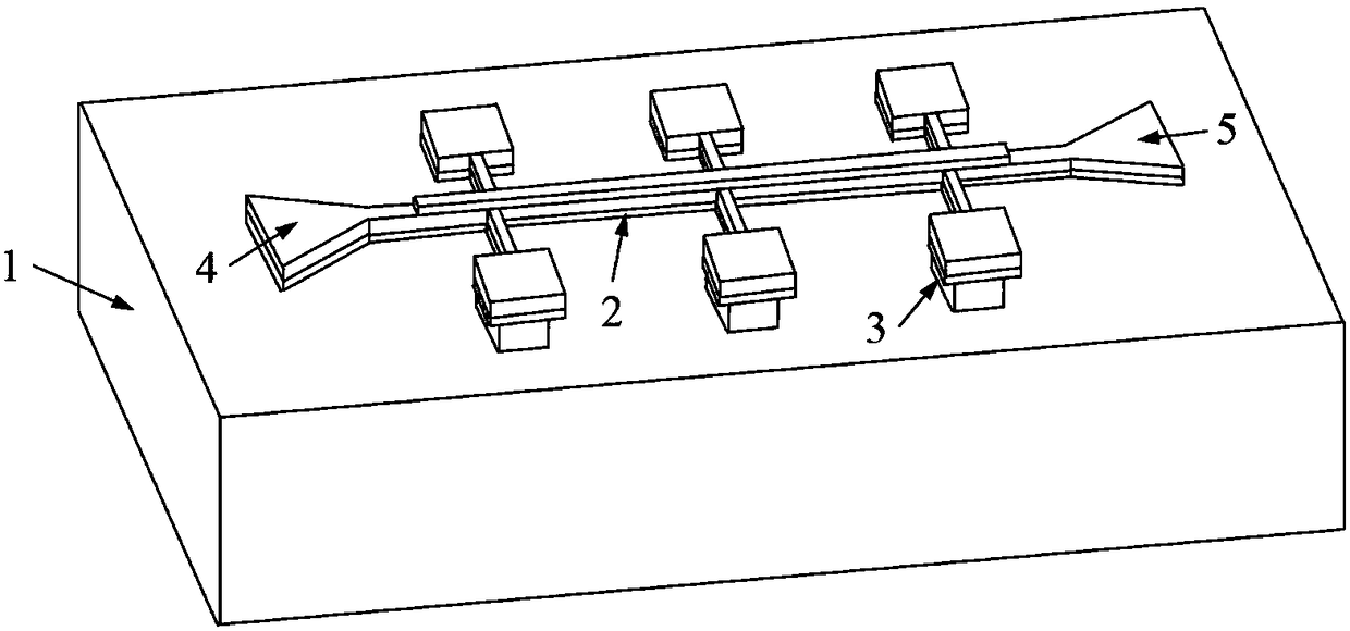
[0047] Constructed as figure 1 The waveguide grating filter shown.

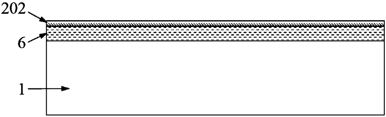
[0048] Using a section structure such as figure 2 The SOI wafer shown has a silicon material substrate 1 , an intermediate layer of silicon dioxide 6 and a top layer of silicon 202 .

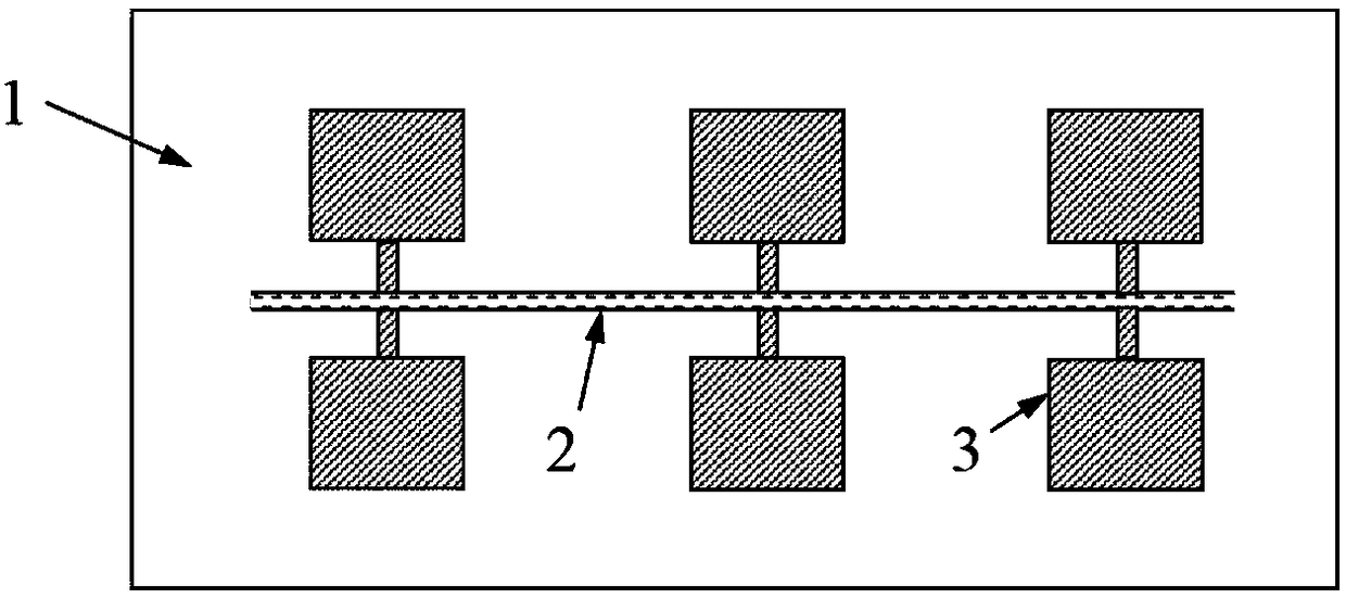
[0049] Spin-coat photoresist on the top silicon of the SOI wafer, and use this as a mask to etch to obtain the waveguide 2 and the beam-column structures 3 arranged periodically on both sides of the waveguide. The top view structure is as follows image 3 shown. Then, for the SOI wafer with the above structure, use hydrofluoric acid (HF) wet etching to remove the silicon dioxide layer under the ridge waveguide, and keep part of the silicon dioxide as the pillar 302a, to obtain the following: Figure 4 The structure shown with an air gap, also constitutes a beam-column structure.

[0050] The waveguide body 202, the optical input end 4 and the optical input end 5 are all coupler structures fabricated on the top silicon layer ...


PUM

PropertyMeasurementUnit
heightaaaaaaaaaa
thicknessaaaaaaaaaa
lengthaaaaaaaaaa

Abstract

The invention provides a waveguide grating filter. The waveguide grating filter comprises a substrate (1) and a waveguide (2), and further comprises a beam column structure (3) used for supporting thewaveguide (2), wherein the beam column structure (3) comprises column structures (302) and a beam structure (301); the column structures (302) are positioned on two sides of the waveguide (2) and arranged on the substrate (1); the beam structure (301) is used for connecting the column structures (302); an air gap (201) is formed between the waveguide (2) and the substrate (1). According to the waveguide grating filter disclosed by the invention, spectral characteristics of the waveguide grating filter are changed by adopting a thermal tuning method, a local thermal isolation structure betweenthe waveguide and the substrate is realized by forming the air gap below the waveguide, and vertical mobility of the heat is obstructed, so that the power consumption of the waveguide grating filteris reduced. The waveguide grating filter disclosed by the invention has the advantages of being low in power consumption, high in tuning efficiency, fast in tuning, stable in structure, easy to integrate and the like, and has obvious application value in a wavelength division multiplexing system.

Description

【Technical field】 [0001] The invention belongs to the technical field of optical filtering, relates to the technical field of integrated optical waveguide devices, in particular to a waveguide grating filter and a manufacturing method thereof. 【Background technique】 [0002] Optical filter is an important photonic device, which is mainly used in the integrated optical circuit where the silicon-on-insulator (SOI) substrate is the optical platform. The main function of the optical filter is to frequency-separate the light containing multiple frequency components to obtain one or more frequency components. In the framework of optical communication systems, filters mainly include Fabry-Perot (F-P) filters, Mach-Zehnder (MZ) filters, grating filters, and microring filters. Compared with the other three structures, the grating filter has the advantages of simple fabrication and easy design of spectral characteristics, and has received extensive attention. [0003] Tunable wavegu...

Claims


Application Information

Patent Timeline
Patent Type & Authority Applications(China)
IPC IPC(8): G02B6/12G02B6/138G02F1/01
CPCG02B6/12033G02B6/138G02F1/0147
Inventor 陈开段飞余永林
Owner HUAZHONG UNIV OF SCI & TECH
Why Eureka
Try Eureka