Request handling method of 3D MLC flash device

A technology for request processing and equipment, applied in electrical digital data processing, information storage, static memory, etc., can solve the problem of reducing the number of flash memory device erasures, and achieve the effects of improving read performance, prolonging service life, and shortening latency.

Active Publication Date: 2018-09-25
HUAZHONG UNIV OF SCI & TECH
View PDF12 Cites 2 Cited by
  • Summary
  • Abstract
  • Description
  • Claims
  • Application Information

AI Technical Summary

Problems solved by technology

[0004] Aiming at the defects and improvement needs of the prior art, the present invention provides a request processing method for a 3D MLC flash memory device, the purpose of which is to make full use of the 3D MLC flash memory chip, which can interrupt the write / erase operation and dynamically adjust the internal memory of the wafer through advanced commands. The characteristics of the working mode of the flash memory block reduce the delay of garbage collection, so as to alleviate the performance degradation caused by the long garbage collection delay of 3D MLC applied in the solid state disk system, and reduce the number of times of erasing of the flash memory device, thereby Extend the life of your SSD

Method used


Image

  • Request handling method of 3D MLC flash device
  • Request handling method of 3D MLC flash device
  • Request handling method of 3D MLC flash device

Examples


Embodiment Construction

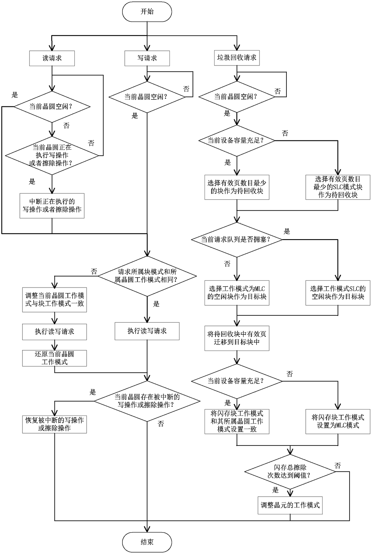
[0041] In order to make the object, technical solution and advantages of the present invention clearer, the present invention will be further described in detail below in conjunction with the accompanying drawings and embodiments. It should be understood that the specific embodiments described here are only used to explain the present invention, not to limit the present invention. In addition, the technical features involved in the various embodiments of the present invention described below can be combined with each other as long as they do not constitute a conflict with each other.

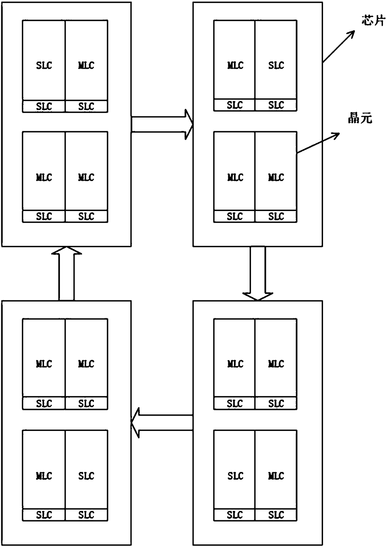
[0042] The read and write operation granularity of the 3D MLC flash memory chip is page, and the erase operation granularity is block. One chip contains multiple wafers, one wafer contains multiple blocks, and one block contains multiple pages. The 3D MLC flash memory adopted in this embodiment In the chip, the size of a block is 1024 pages, each flash memory chip contains 4 wafers, and each waf...


PUM


Abstract

The invention discloses a request handling method of a 3D MLC flash device. The method comprises the following steps: performing a read request by a read request fir mode; performing a write request while a wafer is idle; ensuring that the working mode of the related wafer is consistent with the working mode of the related block during performing the read / write request; performing trash recoveryrequest while the wafer is idle; selecting the block with the least active pages in the block under an SLC mode as the block to be recovered in case of insufficient current capacity of the device; selecting an idle block of the SLC mode as a target block in case of jam in current array of the device; setting the wiped working mode of the block to be recovered as the MLC mode in case of insufficient current capacity of the device; and circularly setting the working mode of the next wafer as the SLC mode in case that the total wiping quantity of all wafers is certainly increased. According to the method, the new properties of a 3D MLC flash chip can be fully utilized, so that the delay time in trash recovery can be decreased, and the service life of the flash device is prolonged.

Description

technical field [0001] The invention belongs to the field of SSD (Solid State Disk, solid state disk, solid state disk for short) storage control, and more specifically relates to a request processing method of a 3D MLC flash memory device. Background technique [0002] Due to its advantages in performance and energy consumption, flash memory is widely used in scenarios such as personal computers, servers, and data centers. However, NAND flash memory has reached its physical limit when the process is less than 20nm, and many flash memory manufacturers have shifted their development focus to 3D flash memory. Compared with 2D flash memory, 3D flash memory has higher density and lower price. 3D flash memory chips also provide more advanced command support. First of all, the 3D flash memory chip can interrupt the writing operation or erasing operation being performed on the chip, and resume the previous writing operation or erasing operation after performing other operations. ...

Claims


Application Information

Patent Timeline
Patent Type & Authority Applications(China)
IPC IPC(8): G06F12/02G11C16/16
CPCG06F12/0253G11C16/16
Inventor 童薇冯丹刘景宁李帅冯雅植
Owner HUAZHONG UNIV OF SCI & TECH
Why Eureka
Try Eureka