Package stack structure and manufacturing method thereof

A technology of packaging stacking and packaging structure, which is applied in semiconductor/solid-state device manufacturing, semiconductor/solid-state device components, semiconductor devices, etc., can solve the problems of increasing the thickness of the overall stacked packaging structure and manufacturing costs, and improve product yield. , the effect of reducing size and manufacturing cost

Active Publication Date: 2019-10-11
POWERTECH TECHNOLOGY INC
View PDF4 Cites 0 Cited by
  • Summary
  • Abstract
  • Description
  • Claims
  • Application Information

AI Technical Summary

Problems solved by technology

However, the interposer between different layers of packaging units increases the thickness and manufacturing cost of the overall stacked package structure

Method used


Image

  • Package stack structure and manufacturing method thereof
  • Package stack structure and manufacturing method thereof
  • Package stack structure and manufacturing method thereof

Examples


Embodiment Construction

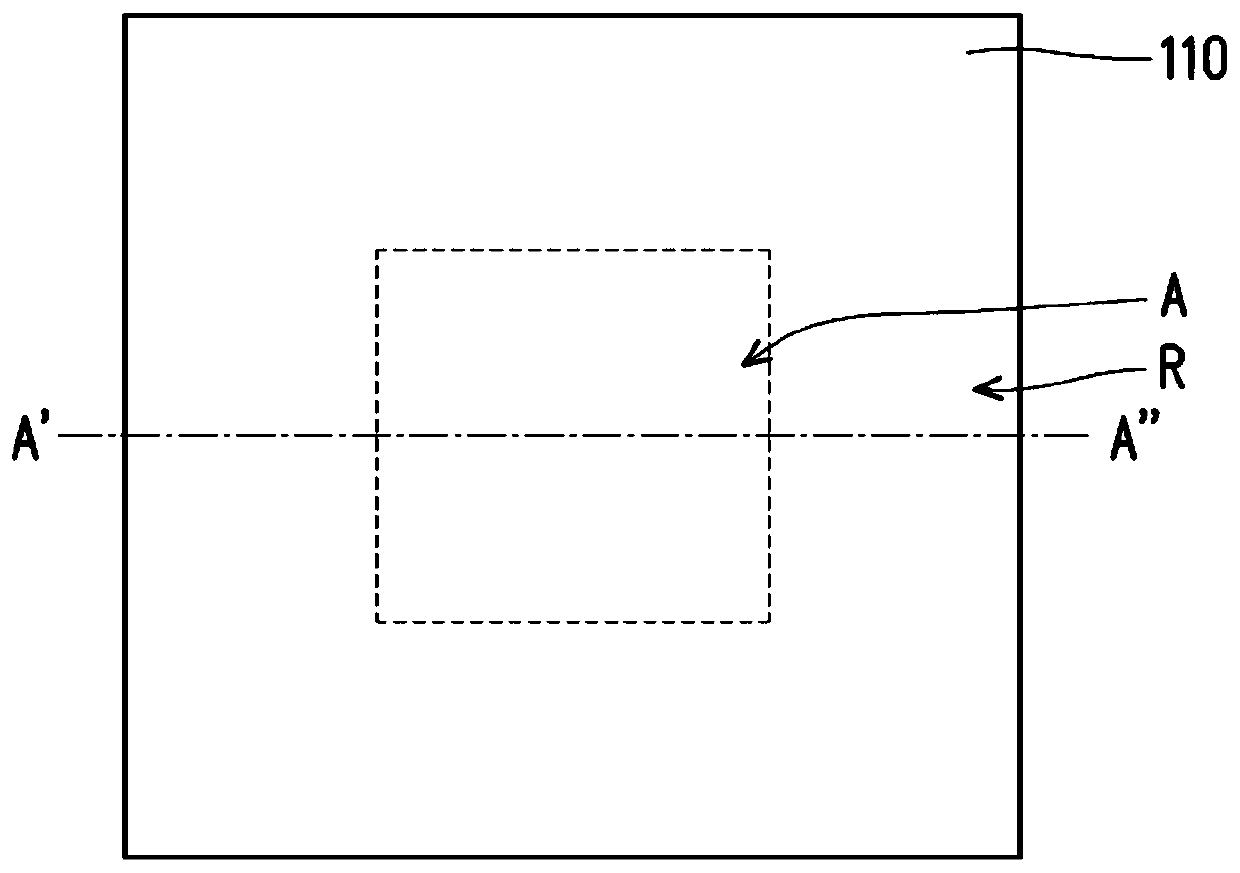
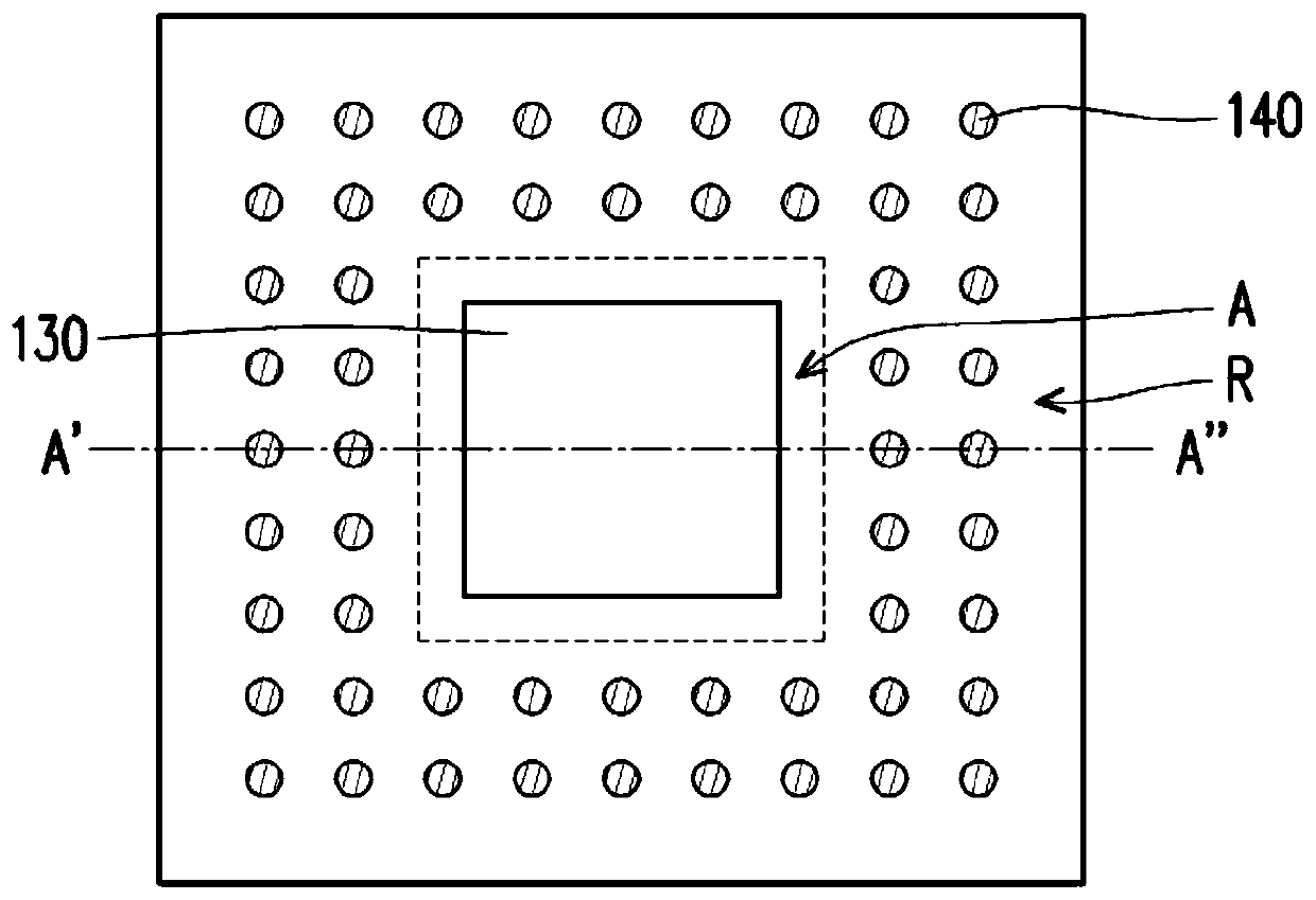
[0060] Figure 1A to Figure 1G is a simplified top view of the manufacturing process of a package stack structure 10 according to an embodiment of the present invention. Figure 2A to Figure 2G is along Figure 1A to Figure 1G The cross-sectional schematic diagram of the section line A'-A", Figure 2H is along Figure 1G The cross-sectional schematic diagram of the section line B'-B".

[0061] Please refer to Figure 1A and Figure 2A ,in Figure 1A omitted to show Figure 2AThe first circuit layer 114 in. Firstly, a first carrier 110 is provided. The first carrier 110 has a first surface S1 and a second surface S2 opposite to the first surface S1 . The first carrier 110 includes a first core layer 112 , a first wiring layer 114 on the first surface S1 , a second wiring layer 116 on the second surface S2 , and a plurality of via holes 118 . The first core layer 112 is the middle layer of the first carrier 110, and its material includes, for example, glass, epoxy resin,...


PUM


Abstract

The invention provides a package stack structure including a first package structure and a second package structure. The first package structure includes a first carrier plate, a first chip, a first insulating sealing body, a conductive structure, a seed layer and a circuit layer. The carrier pads, the first chip, the first insulating sealing body and the conductive structure are located on the first surface of the first carrier. The first insulating sealing body includes a first opening and a trench. The first insulating sealing body includes encapsulation glue, fillers and metal salts dispersed in the encapsulation glue. The seed layer includes metal reduced by metal salts, and is arranged on the surface of the first opening and the trench. The circuit layer is configured on the seed layer. The second packaging structure is electrically connected to the circuit layer. In addition, the present invention also provides a method for manufacturing the package stack structure.

Description

technical field [0001] The present invention relates to a packaging stack structure and a manufacturing method thereof, in particular to a packaging stacking structure using an insulating package with metal salts and a manufacturing method thereof. Background technique [0002] In recent years, as the volume of packages becomes smaller and smaller, the application of multi-chip stacked semiconductor package structures, such as package on package (PoP), also grows rapidly. [0003] In the existing stacked packaging, different chip packaging units are stacked on each other, and an interposer is interposed between these chip packaging units. For example, memory chip packaging units are stacked on the interposer, and logic chip packaging units are stacked on the interposer. However, the interposer between different layers of packaging units increases the thickness and manufacturing cost of the overall stacked packaging structure. Therefore, in order to further reduce the size ...

Claims


Application Information

Patent Timeline
Patent Type & Authority Patents(China)
IPC IPC(8): H01L25/10H01L23/31H01L21/98
CPCH01L23/3128H01L25/105H01L25/50H01L2225/1011H01L2225/1058H01L2224/16225H01L2924/15311H01L2924/181H01L2924/00012
Inventor 陈裕纬徐宏欣王启安
Owner POWERTECH TECHNOLOGY INC
Why Eureka
Try Eureka