
Antenna manufacturing method based on PDS technology, and antenna manufactured through antenna manufacturing method

A manufacturing method and antenna technology, applied in the field of electronic communication, can solve the problems of antenna affecting performance, weak adhesion, cost impact, etc., and achieve the effects of simplifying the printing process, saving the via process, and improving the yield.

Inactive Publication Date: 2018-09-25
SHANGHAI DEMAN ELECTRONICS TECH +1
View PDF4 Cites 1 Cited by
  • Summary
  • Abstract
  • Description
  • Claims
  • Application Information

AI Technical Summary

Problems solved by technology

However, in these existing methods, the antenna is not firmly bonded to materials such as glass, ceramics, zirconia, and sapphire glass, which causes the antenna to drop and affect performance.
[0005] In addition, most of the existing mobile phone antennas (including NFC antennas) are made on the front case, rear case or small bracket. When the company produces the antenna, it needs to obtain the materials and stick the product on the case or through other methods. fabricated on the shell
In this case, the manufacturing process is more complicated and there are many processes
For customers and suppliers, the resulting logistics turnover and complex conventional manufacturing processes all have a greater impact on costs. Therefore, multi-purpose antennas can be produced in a limited space, reducing complex conventional manufacturing processes, and overcoming the current The difficulty of all antenna manufacturing processes, and the fact that the antenna can achieve the most ideal function is the current top priority

Method used


Image

  • Antenna manufacturing method based on PDS technology, and antenna manufactured through antenna manufacturing method
  • Antenna manufacturing method based on PDS technology, and antenna manufactured through antenna manufacturing method
  • Antenna manufacturing method based on PDS technology, and antenna manufactured through antenna manufacturing method

Examples


Embodiment 1

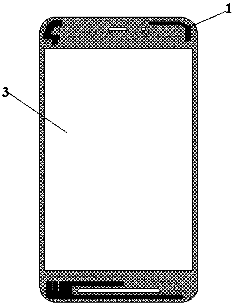
[0044] The antenna manufacturing method based on the PDS process in this embodiment specifically includes the following steps:

[0045] (1) Prepare a bonding ink with strong adhesion;

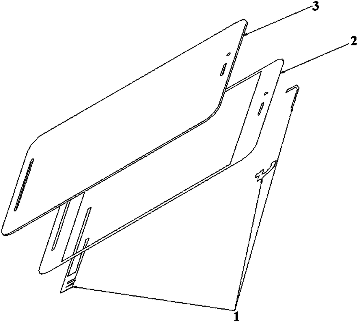
[0046] (2) Pad-print the corresponding built-in antenna 1 circuit onto the glass carrier 3 (PS: the product is a touch screen At this moment, masking ink 2 has been attached to the transparent glass carrier 3);

[0047] (3) Dry at 150°C.

[0048] The adhesive ink with strong adhesive force adopted in the above steps comprises the following components in parts by weight: 35 parts of basic resin acrylic resin (Acryl resin); 10 parts of auxiliary resin isocyanate resin (Isocyanate resin); 1.2 parts of adhesive; 1.2 parts of thickener; 32 parts of organic solvent benzene. The above-mentioned bonding ink can be prepared by conventional methods. The following method can be used to prepare the raw materials according to the above ratio, then mix the raw materials, stir and mix them uniformly a...

Embodiment 2

[0057] The antenna manufacturing method based on the PDS process in this embodiment specifically includes the following steps:

[0058] (1) Prepare a bonding ink with strong adhesion;

[0059] (2) Screen-print the corresponding built-in antenna 1 circuit onto the glass carrier 3 (PS: the product is a touch screen At this moment, masking ink 2 has been attached to the transparent glass carrier 3);

[0060] (3) Dry at 120°C.

[0061] The reliability test result is consistent with Example 1; the cost advantage is equivalent to that of Example 1, and more ink will be wasted relative to pad printing; the ink with strong adhesion used in the above steps is consistent with Example 1.

Embodiment 3

[0063] The antenna manufacturing method based on the PDS process in this embodiment specifically includes the following steps:

[0064] (1) Prepare a bonding ink with strong adhesion;

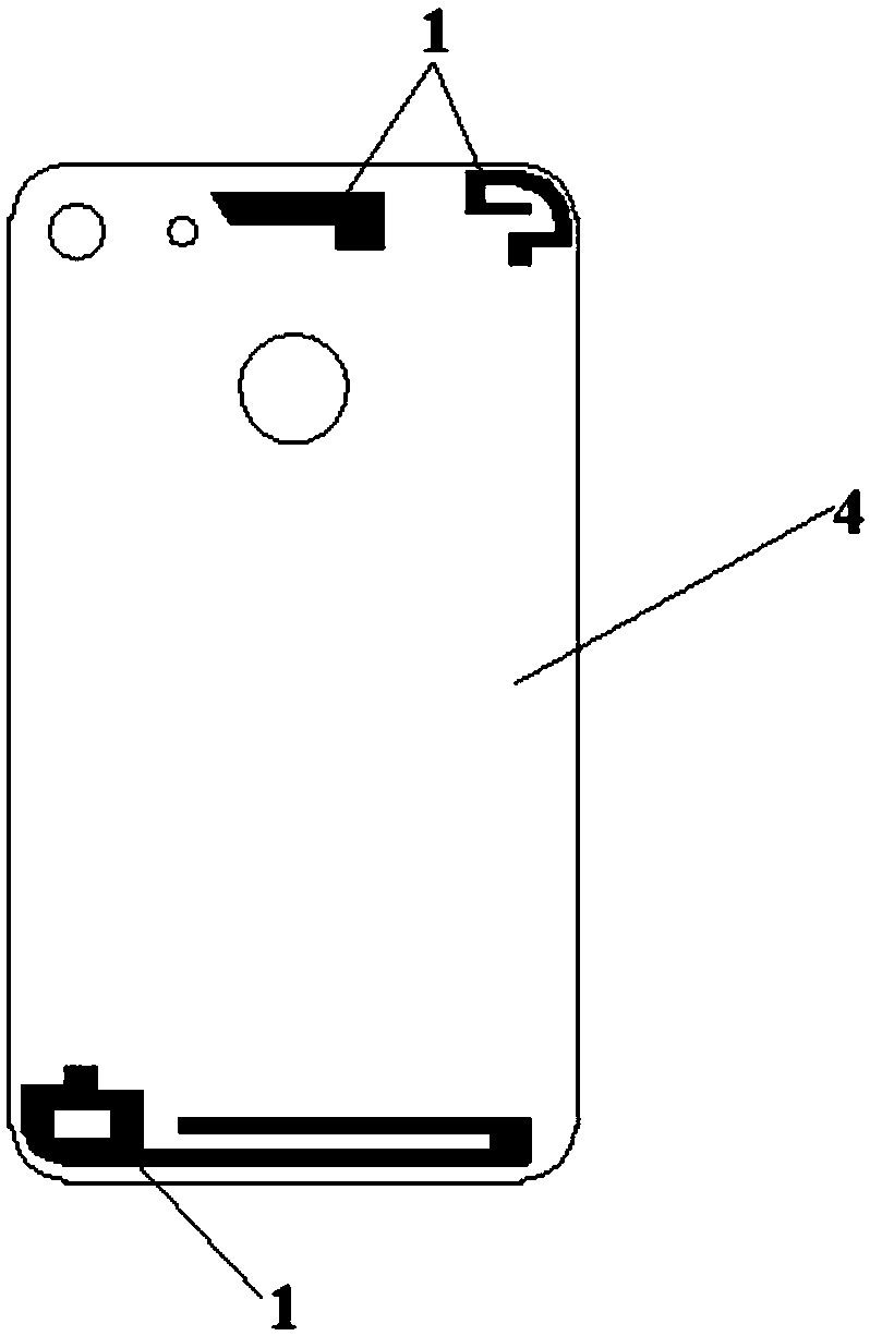
[0065] (2) Print the corresponding built-in antenna 1 circuit on the ceramic back cover 4 (such as Figure 3-4 shown);

[0066] (3) Dry at 160°C.

[0067] The adhesive ink with strong adhesion used in the above steps includes the following components in parts by weight: 36 parts of basic resin acrylic resin (Acryl resin); 9 parts of auxiliary resin isocyanate resin (Isocyanate resin); 1.3 parts of adhesive; 1.4 parts of thickener; 31 parts of organic solvent benzene. The above-mentioned bonding ink can be prepared by conventional methods. The following method can be used to prepare the raw materials according to the above ratio, then mix the raw materials, stir and mix them uniformly at a high speed, and then grind to make the fineness below 15um to obtain the adhesive ink with s...


PUM


Abstract

The invention relates to an antenna manufacturing method based on the PDS technology, and an antenna manufactured through the antenna manufacturing method. The method comprises the following steps: blending adhesive ink which is suitable for the coating of a glass or ceramic carrier; enabling a built-in NFC antenna circuit to be printed on the glass or ceramic carrier coated with the adhesive ink;performing the drying under the temperature of 60-250 DEG C, and forming a single-side NFC antenna circuit, thereby completing the manufacturing of the antenna. Compared with the prior art, the method is simple in technological step, does not need via holes, can reduce the working procedures and bad effects caused by the working procedures, saves the cost, improves the yield, can directly employa pogo pin, an elastic piece or a metal steamed bread contact feed point, facilitates the industrial popularization and application, and improves the work efficiency.

Description

technical field [0001] The invention belongs to the technical field of electronic communication, and relates to a method for manufacturing an antenna based on a PDS process and an antenna made by the method. Background technique [0002] Nowadays, the development of electronic products is changing with each passing day, and the functions are becoming more and more powerful, while the products are getting smaller and thinner. As one of the important components of electronic products, the performance and size of antennas are directly related to the quality of electronic products. With the miniaturization of wireless communication products, built-in antennas have gradually replaced external antennas, and have now become the mainstream of antenna design. [0003] For example, in terms of technology: the existing antennas for mobile phones, watches, computers, etc. are usually prepared by the following methods: first, using the flexible printed circuit board (Flexible Printed Cir...

Claims


Application Information

Patent Timeline
Patent Type & Authority Applications(China)
IPC IPC(8): H01Q1/38H01Q1/24
Inventor 柯栎炎张平杨帆方永莉
Owner SHANGHAI DEMAN ELECTRONICS TECH
Learn More