Display device and preparation method thereof
A display device and display module technology, which is applied in semiconductor/solid-state device manufacturing, electrical components, electric solid-state devices, etc., can solve problems such as poor water-oxygen barrier performance, achieve performance improvement, increase mechanical strength, and avoid breakage Effect
- Summary
- Abstract
- Description
- Claims
- Application Information
AI Technical Summary
Problems solved by technology
Method used
Image
Examples
Embodiment 1
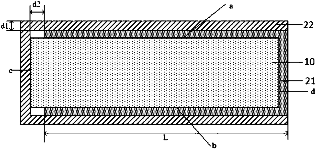
[0047] An embodiment of the present invention provides a display device, such as figure 2 shown. Among them, the display module is described by taking a cube structure and a film barrier layer covering the four sides of the display module as an example, and the four sides of the cube display module are defined as the top surface a, the bottom surface b, and the top surface The first direction side c and the second direction side d between a and the bottom surface b. The display device includes a display module 10, and a film barrier layer composed of several barrier films (such as a first barrier film 21 and a second barrier film 22). Wherein, each barrier film covers three consecutive adjacent surfaces of the display module 10; the film barrier layer composed of all barrier films covers the display module 10 to form a closed cavity, and the display module 10 is arranged in the cavity .
[0048] Among them, the material of the barrier film can be an inorganic dielectric ma...
Embodiment 2
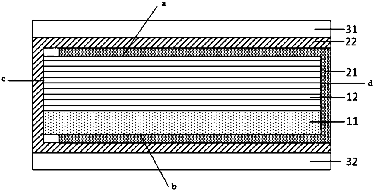
[0071] An embodiment of the present invention provides a display device, such as Figure 4 As shown, the difference from Example 1 is that the first barrier film 21 and the second barrier film 22 are intersected, that is, the first barrier film 21 covers one surface of the second barrier film 22, and the second barrier film 22 covers the second barrier film 22. One side of a barrier film 21.
Embodiment 3
[0073] An embodiment of the present invention provides a method for manufacturing a display device, such as Figure 5 shown, including the following steps:
[0074] Step S11, forming a display module on the substrate.
[0075] Step S12, a layer of barrier film is adhered to at least one surface of the display module.
[0076] Wherein, a layer of barrier film can be attached to one surface of the display module 10 , or a layer of barrier film can be attached to multiple surfaces of the display module 10 at the same time. For example, a barrier film may be laminated on the top surface and the corresponding bottom surface of the display module 10 .
[0077] Step S13 , bending the barrier film along the edge of the surface of the display module to cover at least two consecutive adjacent surfaces of the display module, wherein the consecutive adjacent surfaces are not in the same plane.
[0078]After a layer of barrier film is attached to one surface of the display module 10, th...
PUM
 Abstract
Description
Claims
Application Information
 - R&D
- Intellectual Property
- Life Sciences
- Materials
- Tech Scout
- Unparalleled Data Quality
- Higher Quality Content
- 60% Fewer Hallucinations
Browse by: Latest US Patents, China's latest patents, Technical Efficacy Thesaurus, Application Domain, Technology Topic, Popular Technical Reports.
© 2025 PatSnap. All rights reserved.Legal|Privacy policy|Modern Slavery Act Transparency Statement|Sitemap|About US| Contact US: help@patsnap.com


