PCB rubberizing method

A kind of PCB board and glue technology, which is applied in the direction of PCB tool positioning, electrical components, and simultaneous processing of multiple printed circuits. and other problems, to achieve the effect of high patch efficiency, easy fixing, and guaranteeing the yield of the patch

Pending Publication Date: 2018-09-28
SHENZHEN BAOMING TECH
View PDF0 Cites 4 Cited by
  • Summary
  • Abstract
  • Description
  • Claims
  • Application Information

AI Technical Summary

Problems solved by technology

However, some electronic devices, such as the FPC board of the light bar in the mobile phone, due to the small shape of the light bar and the requirement of thinning the mobile phone, the space left for the connection of the light bar in the mobile phone is very small, and it is impossible to fix it with screws. Light strips also require heat dissipation, so mobile phone light strips are generally glued together
It is also due to the narrow space where the mobile phone light bar is attached and the light bar is relatively narrow. It is very easy to stick to the wrong side when the adhesive is used, and the mobile phone light bar is also thin. It is very easy to make the PCB board of the light bar or The LED lamp is damaged, so the sticking deviation is more scrapped and the loss is larger

Method used


Image

  • PCB rubberizing method
  • PCB rubberizing method
  • PCB rubberizing method

Examples


Embodiment 1

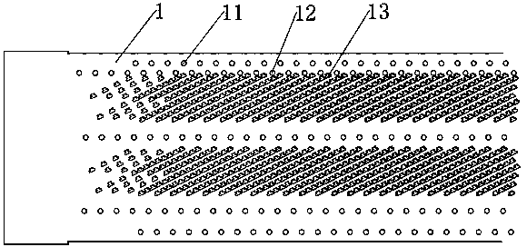
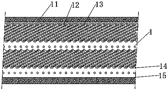
[0026] refer to Figure 1~Figure 6 , a method for sticking glue on a PCB, comprising the following specific steps:

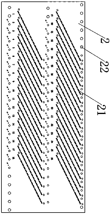
[0027] S1. Refer to image 3 , The whole PCB board production, making the whole PCB board including multiple single boards; during production, the layout of each PCB single board on the whole PCB board is arranged according to the shape of the PCB single board, so as to improve the utilization rate of PCB materials as much as possible . According to the layout, make the whole PCB board 2 and then complete the subsequent steps after patching and welding components. Using the method of patch welding first and then completing the subsequent steps, it can be patched on a large PCB entire board, and the patching efficiency is high. And when welding, the large whole board is easy to fix on the jig and is not easy to deform. In addition, it avoids the high temperature damage of the adhesive strip when bonding first and then welding. The specific placement and welding...


PUM


Abstract

The invention discloses a PCB rubberizing method. The method is characterized by comprising the specific steps of S1, performing manufacturing of a whole PCB, and manufacturing the whole PCB comprising multiple single boards; S2, performing connected film punching, punching an alignment hole and an avoidance hole in the connected film by a hardware die according to the appearance design of the whole PCB, wherein each connected film comprises multiple units corresponding and consistent to the PCB; S3, performing edge cutting on each connected film, and carrying out edge cutting treatment on theconnected film according to the set appearance through a cutter die; S4, performing lamination of each film and the PCB, and enabling each connected film to be aligned to and laminated on the whole PCB; and S5, performing PCB punching, and cutting the rubberized whole PCB into single PCBs. By virtue of the method, the rubberizing yield of the PCB is improved.

Description

technical field [0001] The invention relates to the technical field of PCB board installation methods, in particular to a method for pasting glue on a PCB board. Background technique [0002] PCB (Printed Circuit Board), the Chinese name is printed circuit board, also known as printed circuit board, is an important electronic component, a support for electronic components, and a carrier for electrical connection of electronic components. The devices need to be soldered in the circuit of the PCB board to realize the electrical function. The PCB board soldered with electronic components must be fixed in the electronic equipment, and for some equipment, it can be directly fixed by screws. However, some electronic devices, such as the FPC board of the light bar in the mobile phone, due to the small shape of the light bar and the requirement of thinning the mobile phone, the space left for the connection of the light bar in the mobile phone is very small, and it is impossible to...

Claims


Application Information

Patent Timeline
Patent Type & Authority Applications(China)
IPC IPC(8): H05K3/00
CPCH05K3/0008H05K3/0097
Inventor 张春丁清辉
Owner SHENZHEN BAOMING TECH
Why Eureka
Try Eureka