Variable doped GaN nanowire array photocathode and preparation method thereof

A nanowire array and photocathode technology, which is applied in the manufacture of light-emitting cathodes, photoemission cathodes, nanotechnology, etc., can solve the problems of long transport distances and high emissivity of photoelectrons, so as to improve photoemission quantum efficiency and increase photocurrent , Improve the transport efficiency in the body and the effect of surface escape probability

Inactive Publication Date: 2018-10-09
NANJING UNIV OF SCI & TECH
View PDF3 Cites 10 Cited by
  • Summary
  • Abstract
  • Description
  • Claims
  • Application Information

AI Technical Summary

Problems solved by technology

[0005] The invention proposes a variable-doped GaN nanowire array photocathode, which solves

Method used


Image

  • Variable doped GaN nanowire array photocathode and preparation method thereof
  • Variable doped GaN nanowire array photocathode and preparation method thereof

Examples


preparation example Construction

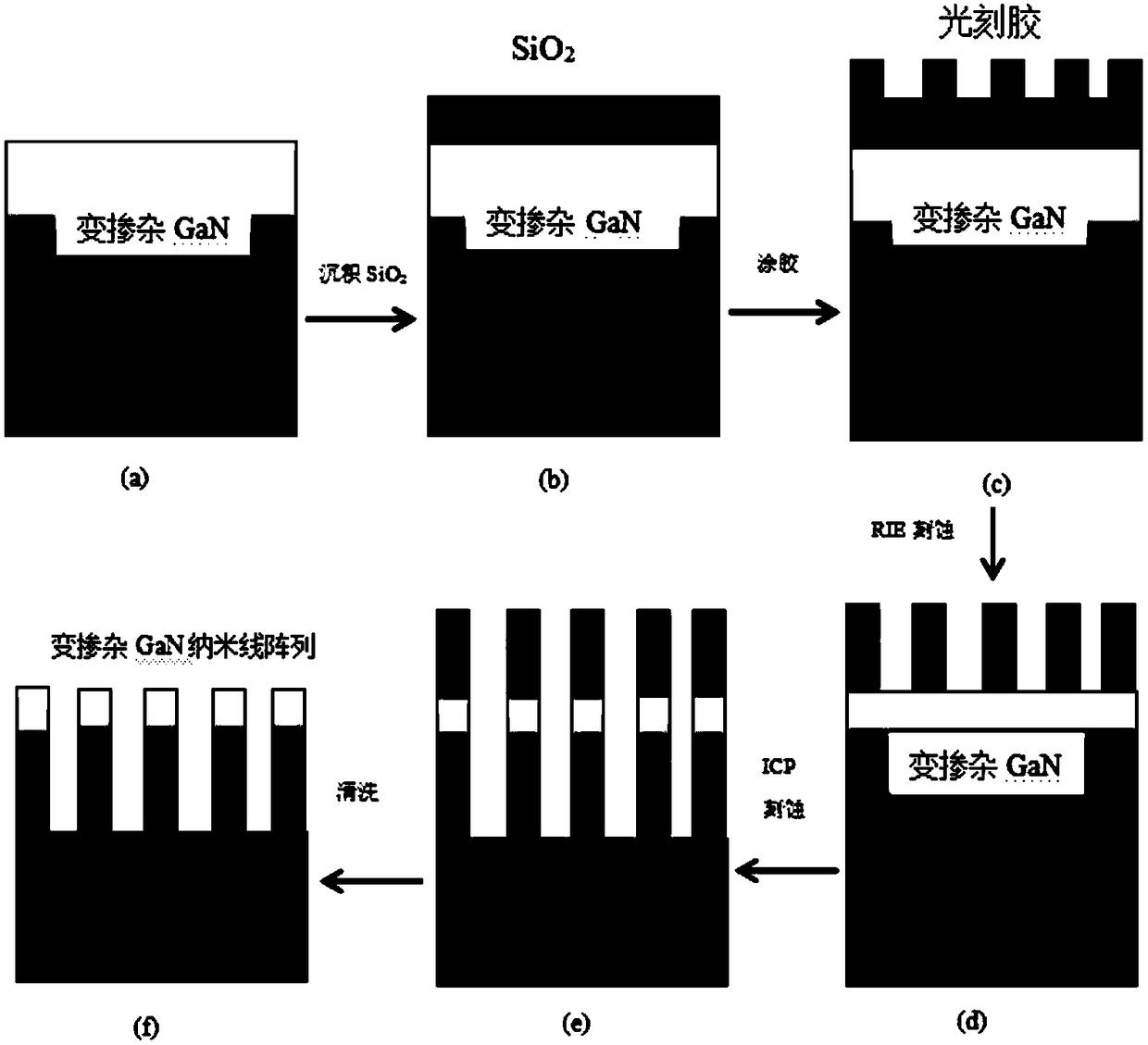
[0027] combine figure 2 As shown, a method for preparing a variable doped GaN nanowire array photocathode, the specific steps are:

[0028] Step 1. On the surface of the substrate, an AlN buffer layer is grown by an MOCVD growth process;

[0029] In a further embodiment, an AlN buffer layer with a thickness of 100-200 nm is grown by MOCVD.

[0030] Step 2. Epitaxially grow a p-type variable doped GaN film on the AlN buffer layer by MOVCD method and p-type doping process, and deposit SiO on the film by PECVD method 2 Layer as a mask, photolithographic exposure and development;

[0031] In some embodiments, a p-type GaN thin film with a variable doping structure with a total thickness of 5-25 μm is grown on the surface of the AlN buffer layer by MOCVD method and a p-type doping process of GaN material, and the doping element is Mg, The range of doping concentration is controlled within 10 16 ~10 19 cm -3 between, and the concentration gradually decreases from the surface ...

Embodiment 1

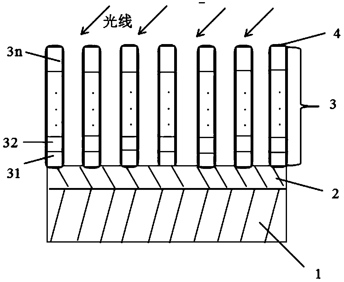
[0044] to combine figure 1 As shown, the variable-doped GaN nanowire array photocathode of the present invention includes a Si substrate 1, an AlN buffer layer 2, a photoemissive layer 3 and a Cs / O active layer 4, and on the surface of the Si substrate layer, a An AlN buffer layer with a thickness of 200nm, and then grow a p-type GaN film with a total thickness variable doping structure on the surface of the AlN buffer layer through the MOCVD method and the p-type doping process of GaN materials, with a thickness of 25 μm, and the variable doping layer It is 15 layers, doped with Mg element, each layer has the same thickness, and the corresponding doping concentration is N 1 , N 2 ,...,N 15 , with a thickness of l 1 The doping concentration N 1 1×10 19 cm -3 , concentration from N 1 to N 15 Gradually decreased, a layer of 2.3μm thick SiO was deposited by PECVD 2 layer as a protective layer, and then coated with a layer of 1.6μm AZ5214 photoresist, after exposure and d...


PUM

PropertyMeasurementUnit
Thicknessaaaaaaaaaa
Diameteraaaaaaaaaa

Abstract

The invention provides a variable doped GaN nanowire array photocathode, comprising a substrate, an AlN buffer layer grown on the substrate, a photoemissive layer grown on the AlN buffer layer, and aCs/O activation layer located on the photoemissive layer, wherein the photoemissive layer is a p-type GaN nanowire array composed of a plurality of equally spaced p-type doped GaN nanowires, and the doping concentration of the p-type doped GaN nanowires gradually decreases from the surface of the buffer layer to the outside. By adopting the variable doped structure having the doping concentrationdecreasing from the surface of the buffer layer to the outside, a built-in electric field for helping in transporting photoelectrons to the surface can be generated in the photocathode of the GaN nanowire array, so that the internal transport efficiency and surface escape probability of photoelectrons are improved, and the photoemissive quantum efficiency of the photocathode is ultimately improved.

Description

technical field [0001] The invention belongs to the technical field of photoelectric emission materials, and in particular relates to a variable-doped GaN nanowire array photocathode and a preparation method thereof. Background technique [0002] A photocathode is a photoemissive material that converts light signals into electrical signals by using the external photoelectric effect. In recent years, with the improvement of GaN material preparation technology, p-type doping technology and the development of ultra-high vacuum technology, GaN photocathode is becoming a new type of high-performance photocathode. The surface of this cathode has a negative electron affinity (NEA). The NEA GaN photocathode has the unique advantages of high quantum efficiency, small dark current, and flexible and adjustable cut-off point. The lack of response band greatly improves the quantum efficiency of the ultraviolet vacuum detection device. [0003] The general GaN photocathode is made of th...

Claims


Application Information

Patent Timeline
IPC IPC(8): H01J1/34H01J9/12B82Y40/00B82Y30/00
CPCH01J1/34B82Y30/00B82Y40/00H01J9/12
Inventor 田健刘磊刁煜陆菲菲
Owner NANJING UNIV OF SCI & TECH
Why Eureka
Try Eureka