GaN photoelectric cathode with superlattice nanowire structure

A photocathode and nanowire technology, which is applied in the direction of photoemission cathode, light-emitting cathode manufacturing, discharge tube main electrode, etc., can solve the problem that the performance of GaN photocathode is difficult to be further improved, so as to improve the photoelectric effect performance and change the quantum efficiency, the effect of improving the quantum efficiency of photoemission

Inactive Publication Date: 2021-10-29
UNIV OF ELECTRONICS SCI & TECH OF CHINA
View PDF6 Cites 0 Cited by
  • Summary
  • Abstract
  • Description
  • Claims
  • Application Information

AI Technical Summary

Problems solved by technology

However, with the progress of research, it is difficult to improve the performance of GaN photocathode by changing the substrate, material structure, thickness, and doping concentration. At present, the performance of GaN photocathode with traditional structure is difficult to be further improved.

Method used


Image

  • GaN photoelectric cathode with superlattice nanowire structure
  • GaN photoelectric cathode with superlattice nanowire structure

Examples


Embodiment Construction

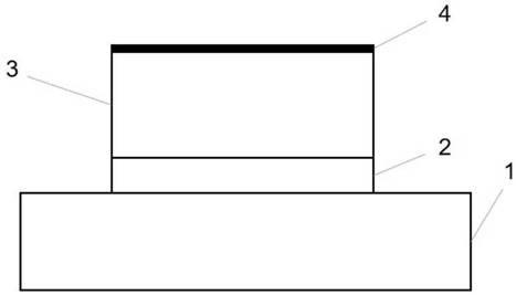
[0020] combine figure 1 , the present invention has a GaN photocathode with a superlattice nanowire structure, which consists of Al from top to bottom 2 o 3 It consists of a substrate layer (1), an AlN buffer layer (2) grown on the substrate, a p-type superlattice AlGaN / GaN nanowire electron emission layer (3) and a Cs / O active layer (4).

[0021] In a further embodiment, the substrate is double-polished sapphire with a thickness of 500 μm.

[0022] In a further embodiment, the thickness of the AlN buffer layer is 50nm.

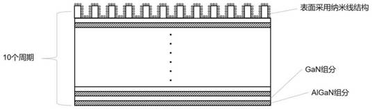
[0023] In a further embodiment, the p-type AlGaN / GaN superlattice nanowire is cylindrical, the superlattice has 10 periods, the thickness of the AlGaN layer in each period is 8 nm, and the thickness of the GaN layer is 8 nm.

[0024] In a further embodiment, the diameter of the p-type AlGaN / GaN superlattice nanowires is 3 nm, and the distance between adjacent doped GaN nanowires is 5 nm.

[0025] In a further embodiment, the hole concentration after dopin...


PUM

PropertyMeasurementUnit
thicknessaaaaaaaaaa
thicknessaaaaaaaaaa
thicknessaaaaaaaaaa

Abstract

The invention discloses a GaN photoelectric cathode with a superlattice nanowire structure. The photoelectric cathode is composed of an Al2O3 substrate layer (1), an AlN buffer layer (2) growing on the substrate, a p-type superlattice AlGaN/GaN nanowire electron emission layer (3) and a Cs/O activation layer (4), from bottom to top. AlGaN/GaN superlattice nanowires are adopted, AlGaN and GaN materials are designed to alternately grow in the form of thin layers of dozens of nanometers and keep strict periodicity to form a multi-layer film structure, namely, an AlGaN/GaN superlattice is formed, and a nanowire structure is adopted on the surface of the AlGaN/GaN superlattice. The GaN photoelectric cathode with the superlattice nanowire structure can influence the movement of charges in the structure, and can overcome the defects of a traditional film photoelectric cathode at the aspects of photon absorption and electron transport, so that the quantum efficiency is changed, the emission performance of photoelectrons and the response wave band of the photoelectric cathode are improved, and finally, the photoelectric emission quantum efficiency of the GaN photoelectric cathode is improved.

Description

technical field [0001] The invention belongs to the technical field of semiconductors and microelectronic devices, and in particular relates to a GaN photocathode with a superlattice nanowire structure. [0002] technical background [0003] A photocathode is a photoemissive material that converts light signals into electrical signals by using the external photoelectric effect. In recent years, with the development and improvement of GaN material preparation technology and p-type doping technology, GaN photocathode is becoming a new type of high-performance photocathode. GaN is the third-generation semiconductor material, which has the advantages of wide bandgap, high quantum efficiency, good stability, radiation resistance, and corrosion resistance. These characteristics make it suitable for the production of high-frequency, high-power, high-temperature, radiation-resistant, and high-density integrated circuits . Its characteristics in terms of band gap make it suitable fo...

Claims


Application Information

Patent Timeline
Patent Type & Authority Applications(China)
IPC IPC(8): H01J1/34H01J9/12H01J40/06
CPCH01J1/34H01J9/12H01J40/06
Inventor 王晓晖王振营张翔班启沛张世博
Owner UNIV OF ELECTRONICS SCI & TECH OF CHINA
Why Eureka
Try Eureka