Focal plane infrared detector chip, detector and preparation method

An infrared detector and focal plane technology, applied in the field of infrared detectors, can solve the problems of application limitation, high cost, limitation of process scalability, etc., and achieve the effect of improving the response band and the absorption rate.

Pending Publication Date: 2021-07-16
INST OF SEMICONDUCTORS - CHINESE ACAD OF SCI
View PDF13 Cites 1 Cited by
  • Summary
  • Abstract
  • Description
  • Claims
  • Application Information

AI Technical Summary

Problems solved by technology

The InAs / GaSb superlattice structure has the advantages of adjustable energy band and flexible control of its cut-off wavelength, but its cost is high, and its application in the civilian field is limited
The cost of the InP / InGaAs system has been relatively reduced, but the InP substrate lattice-matched In 0.53 Ga 0.47 The wavelength range of As / InP detectors is limited to 1.3 μm ~ 1.5 μm, and there are also limitations in process scalability

Method used


Image

  • Focal plane infrared detector chip, detector and preparation method
  • Focal plane infrared detector chip, detector and preparation method
  • Focal plane infrared detector chip, detector and preparation method

Examples


Embodiment Construction

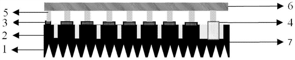
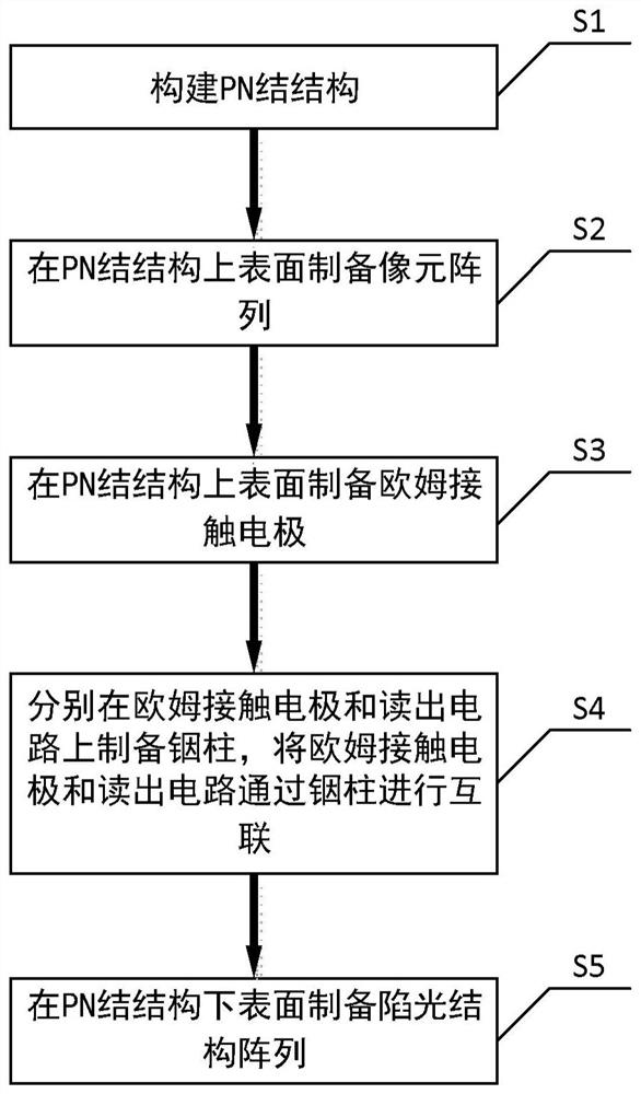
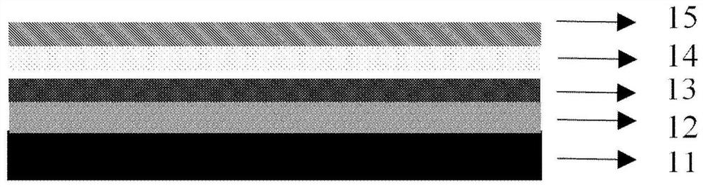
[0036] In order to make the object, technical solution and advantages of the present invention clearer, the present invention will be further described in detail below in conjunction with specific embodiments and with reference to the accompanying drawings.

[0037] It should be understood, however, that these descriptions are exemplary only and are not intended to limit the scope of the present invention. In the following detailed description, for purposes of explanation, numerous specific details are set forth in order to provide a thorough understanding of the embodiments of the invention. It may be evident, however, that one or more embodiments may be practiced without these specific details. In addition, in the following description, descriptions of known technologies are omitted to avoid unnecessarily confusing the concept of the present invention.

[0038] The terminology used herein is for the purpose of describing particular embodiments only, and is not intended to b...


PUM


Abstract

The invention discloses a focal plane infrared detector chip, which comprises a contact layer provided with a first ohmic contact electrode and a pixel array, and a light trapping structure array arranged under the contact layer, wherein each pixel of the pixel array is provided with a second ohmic contact electrode, each second ohmic contact electrode is provided with an indium column, the indium columns are connected with the reading circuit, the doping types of the pixel array, the contact layer and the first ohmic contact electrode are the same, and the contact layer and the second ohmic contact electrodes form PN junctions. According to the focal plane infrared detector chip disclosed by the invention, the absorptivity of a sample is improved, an absorption spectrum covers visible to short wave infrared bands, and the response band of the detector chip is improved. The invention further discloses a preparation method of the focal plane infrared detector chip and a focal plane infrared detector.

Description

technical field [0001] The invention relates to the technical field of infrared detectors, in particular to a focal plane infrared detector chip, a detector and a preparation method. Background technique [0002] An infrared detector is a photosensitive device that can convert invisible infrared radiation into a measurable signal. It has a wide range of applications in the fields of military, meteorology, industry, environmental science, and medical diagnosis. Among them, the short-wave infrared detector mainly refers to the response in the range of 0.7-2.5 μm, which is widely used in military and civilian fields such as night vision, ground remote sensing, and security monitoring. It has low cost, small size, and low cooling power consumption. Advantage. On this basis, if the response range can be extended to the visible light band, it will have breakthrough significance in satellite remote sensing image data and other aspects. [0003] At present, the material systems us...

Claims


Application Information

Patent Timeline
Patent Type & Authority Applications(China)
IPC IPC(8): H01L31/0232H01L31/109H01L27/144H01L31/18G01J5/22
CPCH01L27/1443H01L27/1446H01L31/02327H01L31/109H01L31/184G01J5/22Y02P70/50
Inventor 郝宏玥徐应强牛智川王国伟蒋洞微
Owner INST OF SEMICONDUCTORS - CHINESE ACAD OF SCI
Why Eureka
Try Eureka