

Printed circuit board and display device
A printed circuit board, conductive layer technology, applied in printed circuits, circuit devices, printed circuits, etc., can solve the problems of signal reflection, impedance discontinuity, etc.
- Summary
- Abstract
- Description
- Claims
- Application Information
AI Technical Summary
Problems solved by technology
Method used
Image

Examples
Embodiment 1
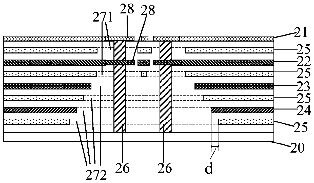
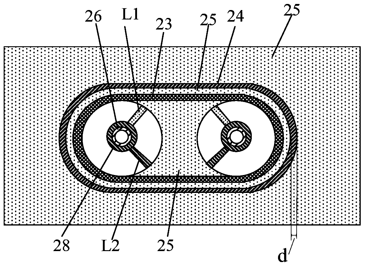
[0028] In order to achieve impedance matching between the signal line and the connection structure, Embodiment 1 of the present invention provides a printed circuit board, figure 2 It is a schematic diagram of the film layer structure of the printed circuit board provided by Embodiment 1 of the present invention, image 3 for figure 2 Bottom view of the film layer above the substrate of the printed circuit board. combine figure 2 and image 3 As shown, the printed circuit board includes insulating and spaced multi-layer conductive layers 21-25 and multiple connection structures 26, the multi-layer conductive layers 21-25 are stacked, and an insulating spacer layer is arranged between every two conductive layers. Each connection structure 26 runs through each conductive layer 21 - 25 , and the connection structure 26 connects the first signal line L1 respectively located in the conductive layer 21 and the second signal line L2 located in the conductive layer 22 . Except ...
Embodiment 2
[0041] Embodiment 2 of the present invention provides a display device, including an array substrate and a printed circuit board connected to the array substrate, and the printed circuit board is the printed circuit board provided in Embodiment 1. Optionally, a driving chip is arranged on the printed circuit board, and the printed circuit board is used to provide a driving signal of the driving chip to the array substrate.
[0042] The display device can be any product or component with a display function such as electronic paper, OLED panel, mobile phone, tablet computer, TV, monitor, notebook computer, digital photo frame, navigator, etc.
[0043] Since the printed circuit board provided by the present invention can realize impedance matching, improve the consistency of impedance during signal transmission, and reduce the signal reflection problem caused by impedance mismatch, therefore, the signal transmitted by the printed circuit board to the array substrate is more accura...
PUM
 Abstract
Description
Claims
Application Information