

Head-mounted device of eyeball tracking device having multi-layer free-form optical waveguide
A head-mounted device and eye-tracking technology, applied in optics, optical components, instruments, etc., can solve problems such as being unfavorable to the simplified design and appearance expansion of the head-mounted device, affecting the effect of eye tracking, and low device integration. , to achieve the effect of solving low device integration, improving user experience, and meeting setting requirements
- Summary
- Abstract
- Description
- Claims
- Application Information
AI Technical Summary
Problems solved by technology
Method used
Image

Examples
Embodiment 1
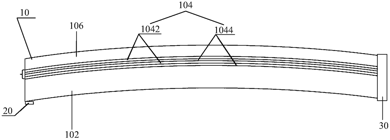
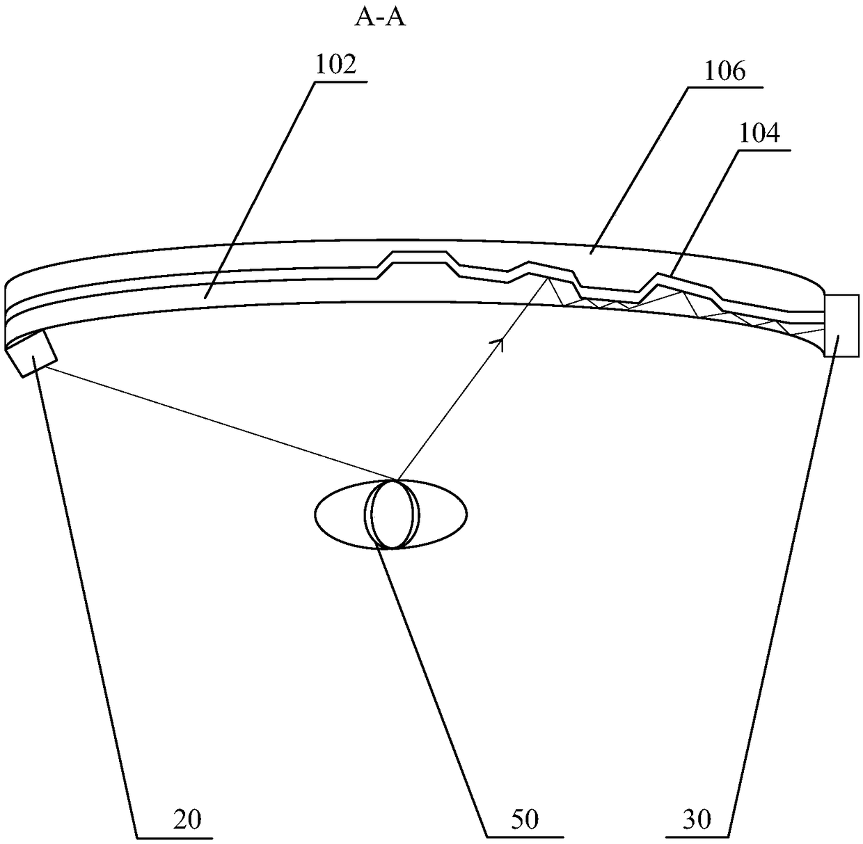
[0074] The contact surfaces of the first-layer optical waveguide 102 and the third-layer optical waveguide 106 with the air space are all arc surfaces, and the interface between the first-layer optical waveguide 102 and the second-layer optical waveguide 104 is a combination of multiple folded surfaces and arc surfaces. The infrared light source 20 is located on the mirror frame on one side of the multilayer free-form surface optical waveguide, and the CMOS element of the eyeball imaging sensor 30 is closely attached to the side of the other side of the multi-layer free-form surface optical waveguide.
[0075] Placing the infrared light source 20 and the CMOS element on different sides of the multilayer free-form surface light wave, changing the shape of the interface between the first layer of optical waveguide 102 and the second layer of optical waveguide 104, can make more light reflected by the eyeball 50 go to the CMOS element. side transmission.
[0076] Infrared light r...
Embodiment 2
[0078] Figure 4 and Figure 5 A schematic structural diagram of an eye tracking device according to an embodiment of the present invention is shown.
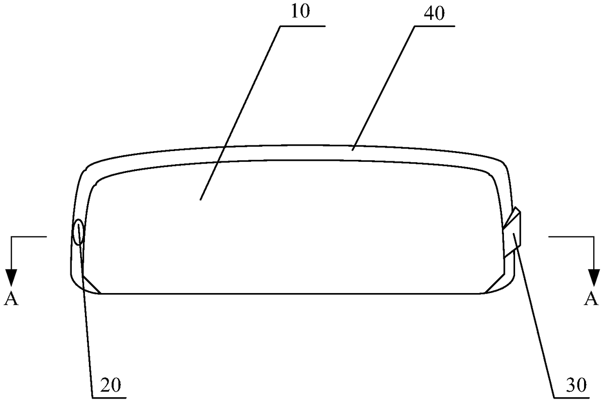
[0079] The outer surface of the first-layer optical waveguide 102 and the outer surface of the third-layer optical waveguide 106 are all configured as arc surfaces, and the interface between the first-layer optical waveguide 102 and the second-layer optical waveguide 104 is configured as a trapezoidal concave surface and an inverted trapezoidal shape. The convex surface is staggered along the width structure direction of the lens 10 to form the second combination structure surface; there are two eyeball imaging sensors 30, which are respectively arranged on both sides of the lens 10, and the eyeball imaging sensor 30 is attached to the side of the corresponding lens 10 ; The infrared light source 20 includes a plurality of infrared light sources 20 distributed on the peripheral contour of the lens 10 . The infrared light sour...
Embodiment 3
[0081] Image 6 and Figure 7 A schematic structural diagram of an eye tracking device according to an embodiment of the present invention is shown.
[0082] In any of the above embodiments, preferably, the outer surface of the first-layer optical waveguide 102 and the outer surface of the third-layer optical waveguide 106 are formed by splicing a plurality of bending planes, the second-layer optical waveguide 104-the third-layer optical waveguide The interface of the waveguide 106 is a combined multi-fold surface. The infrared light source 20 is located on the mirror frame on one side of the multilayer free-form surface optical waveguide, and the CMOS element of the eyeball imaging sensor 30 is closely attached to the side of the other side of the multilayer free-form surface optical waveguide.
PUM
 Abstract
Description
Claims
Application Information