Circuit board connecting structure

A technology for connecting structures and circuit boards, which is applied in the structural connection of printed circuits, printed circuits, printed circuits, etc.

Active Publication Date: 2018-10-16
宁波勇毅科技有限公司
View PDF4 Cites 5 Cited by
  • Summary
  • Abstract
  • Description
  • Claims
  • Application Information

AI Technical Summary

Problems solved by technology

[0003] 1. In the glue bonding method, due to the small contact surface of the two circuit boards, the amount of glue is difficult to control. Too much glue may cause the circuit between the two circuit boards to be disconnected, and the overflow of glue will also cause unsightly appearance. The amount of glue is not enough It will also cause the mechanical connection of the two circuit boards to fail easily; at the same time, due to the physical characteristics of the glue, high temperature will often cause the glue to melt and destroy the bonding effect;
[0004] 2. In the welding method, since the traditional pads and pads are multiple strip metal wires arranged side by side, if the amount of tin is large during welding, tin overflow will cause two or more metal wires arranged side by side. The short circuit is caused by tin conduction between the wires; at the same time, the welding of two circuit boards must undertake the function of electrical transmission while mechanically connecting, so the bonding strength of the bonding material and the substrate bonding material is required to be high during welding; at the same time, the two circuit boards The characteristics of the small contact area of ​​the board have high requirements on the welding technology. Once the welding has problems such as false welding, it will easily lead to the failure of the mechanical connection and the electrical connection.
At the same time, both connection methods greatly limit the optional range of bonding materials

Method used


Image

  • Circuit board connecting structure
  • Circuit board connecting structure
  • Circuit board connecting structure

Examples


Embodiment Construction

[0026] The present invention is described in further detail below in conjunction with accompanying drawing:

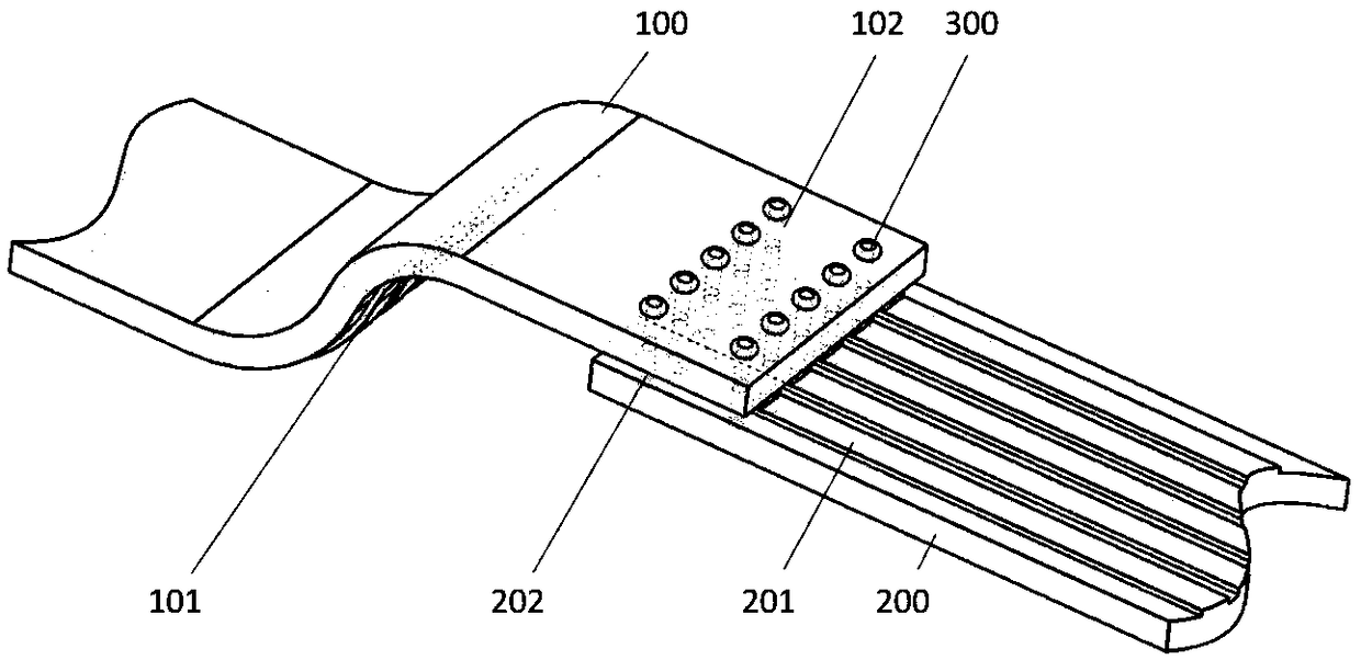
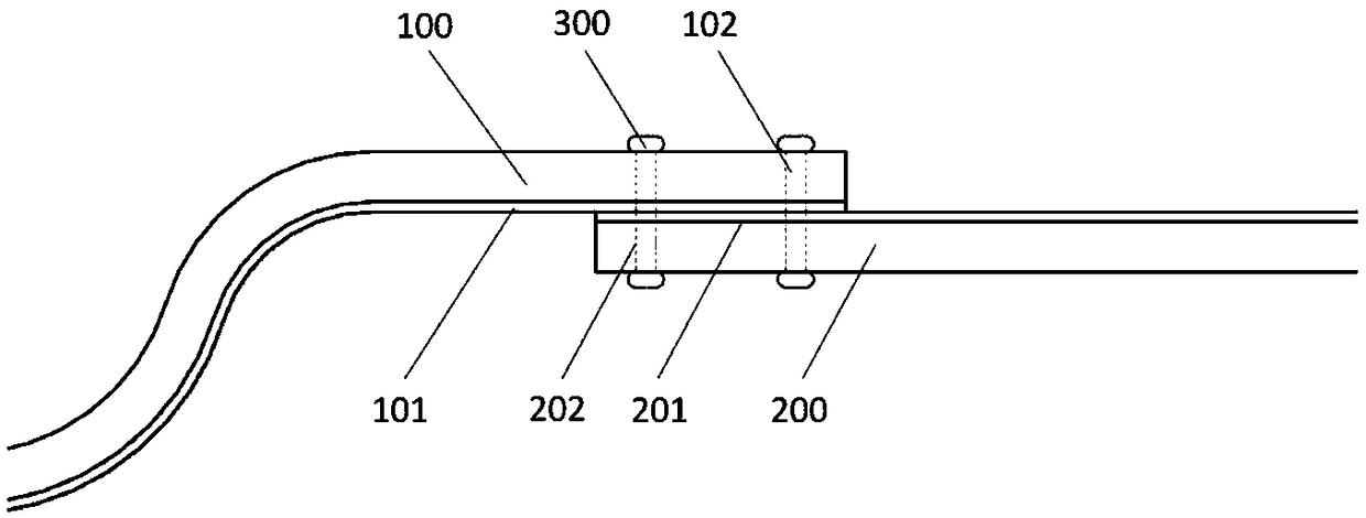
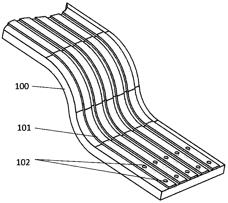
[0027] In the first example herein, figure 1 It is a schematic diagram of the overall structure of an embodiment of a flexible and hard printed circuit board connection structure. It can be seen from the figure that the example of the present invention includes a soft board 100 and a hard board 200, and the two are firmly connected by a pin-shaped structure 300 formed by a bonding material. In the embodiment of the present invention, the bonding material is solder, and the pin-shaped structure 300 formed Formed for solder cooling. The flexible board 100 described in this embodiment is a double-layer circuit board, and the other layer of the circuit board is a physiological indicator monitoring sensor, which is not shown in the figure; the hard board 200 is a double-layer circuit board, and the other layer of the circuit board is for data processing. circuit, not show...


PUM


Abstract

The invention discloses a circuit board connecting structure which comprises a first circuit board and a second circuit board. One of the two circuit boards is a soft board, the other of the two circuit boards is a hard board, or the two circuit boards are both soft boards. A plurality of signal transmission units are arranged on the surface of the first circuit board, through holes are reserved in the ends of the signal transmission units, and the through holes penetrate through the first circuit board and the signal transmission units. Signal transmission units and end through holes corresponding to the first circuit board are arranged on the surface of the second circuit board. The invention discloses a combing method of the circuit boards. Pin-shaped structures with the two ends thicker than the middles are formed in the corresponding through holes of the two circuit boards through combining materials, and firm connection of the two circuit boards is achieved.

Description

technical field [0001] The invention relates to a circuit board connection structure, in particular to a flexible-hard printed circuit board connection structure or a flexible-flexible circuit board connection structure with stable and reliable connection. Background technique [0002] With the development of electronic technology and the continuous improvement of people's requirements for the mobility and portability of electronic products, FPCB (Flexible Printed Circuit Board) can achieve a high degree of integration due to its deformable characteristics, so it is widely used in electronic products. It is becoming more and more widespread, and the traditional PCB (Printed Circuit Board) hard board is still indispensable as the core of electronic products. How to connect the two effectively and beautifully has become an urgent problem to be solved. There are many kinds of connection methods between flexible boards and rigid boards, or between flexible boards and flexible bo...

Claims


Application Information

Patent Timeline
Patent Type & Authority Applications(China)
IPC IPC(8): H05K1/14
CPCH05K1/147H05K2201/10303
Inventor 黎永前毛云龙肖驰王志刚
Owner 宁波勇毅科技有限公司
Why Eureka
Try Eureka