Electronic device junction temperature measurement method and device

A technology of electronic devices and measuring devices, which is applied in the field of semiconductor device junction temperature measurement, can solve problems such as differences, and achieve the effect of simple test principle, simple implementation method, and wide range of effective measurable objects

Pending Publication Date: 2018-10-19
CHINA ELECTRONICS STANDARDIZATION INST
View PDF0 Cites 2 Cited by
  • Summary
  • Abstract
  • Description
  • Claims
  • Application Information

AI Technical Summary

Problems solved by technology

However, both methods have their own limitations. Conventional hybrid circuits and integrated circuits do not have corresponding interfaces to collect their temperature-sensitive parameters; for the indirect method, it is necessary to uncap the device, which is firstly a destructive test, and secondly The junction temperature state of the device after the cap is removed will be different from the real situation without the cap due to thermal radiation and heat convection.

Method used


Image

  • Electronic device junction temperature measurement method and device
  • Electronic device junction temperature measurement method and device
  • Electronic device junction temperature measurement method and device

Examples


Embodiment Construction

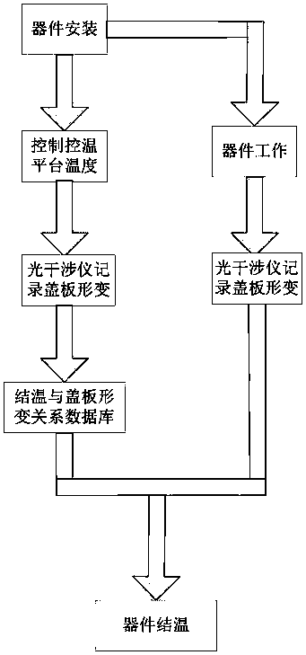
[0030] The present invention will be described in more detail below in conjunction with the accompanying drawings and specific embodiments.

[0031] 1) Construction of junction temperature measurement system

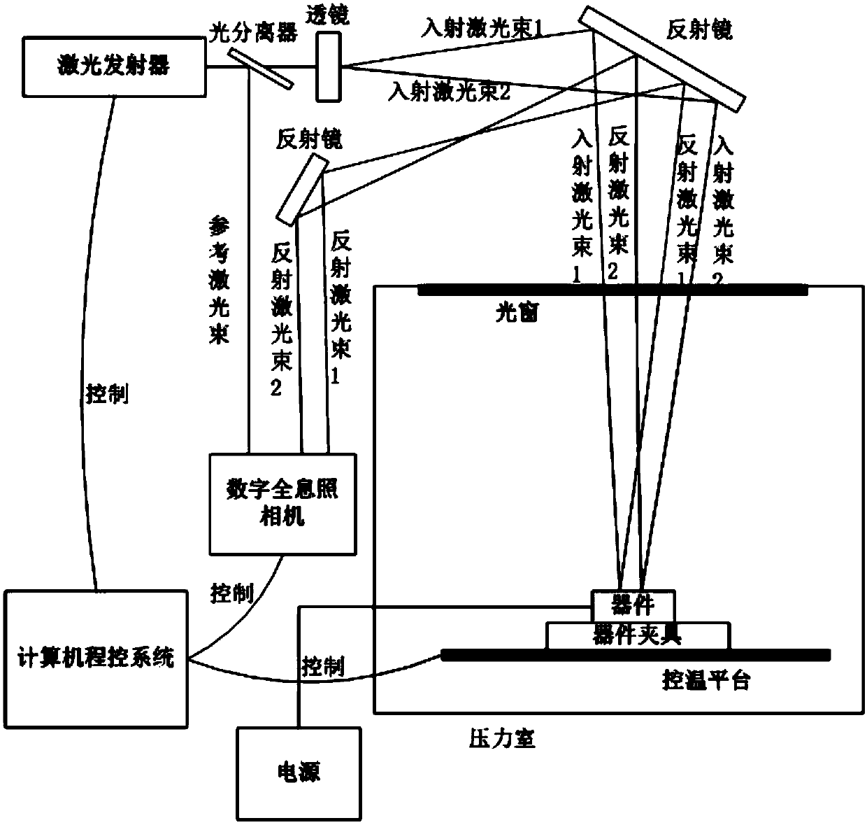
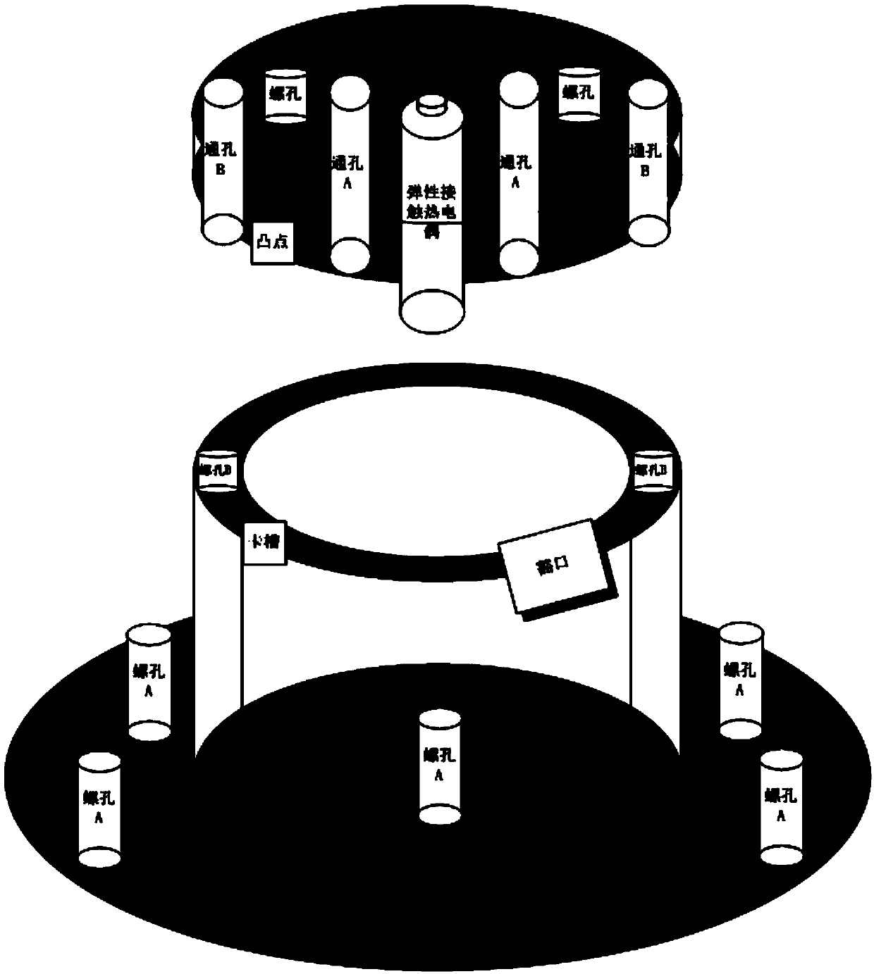
[0032] figure 1 is a schematic diagram of the junction temperature measurement system built as described in this embodiment, as shown in figure 1 As shown, the junction temperature measurement system includes: pressure chamber, laser interferometer, temperature control platform, device fixture, power supply, computer control and calculation system.

[0033] The pressure chamber can ensure the pressure is stable and will not affect the accuracy of the deformation measurement of the cover due to the change of the ambient atmospheric pressure; the laser interferometer records the reference laser beam under different conditions and the laser reflected by the device cover through the digital holographic system The beam forms an interference image, so that the deformation of...


PUM


Abstract

The invention relates to an electronic device junction temperature measurement method and device, belongs to the cover plate junction temperature measurement technology field and mainly utilizes the principle that the internal atmosphere of a device expands with temperature change to cause deformation of a device cover plate to obtain the junction temperature inside the device. The method comprises steps that firstly, the device in a non-working condition is heated, deformation of the device cover plate at each temperature point is monitored by a laser interferometer, so the one-to-one correspondence relationship between the heating temperature (the device junction temperature) and deformation of the device cover plate is obtained; secondly, deformation of the device cover plate is monitored under the working condition of the device and is compared with deformation of the device cover plate under the non-working condition of the device, and the junction temperature of the device can beobtained. The method is advantaged in that the junction temperature of discrete devices, integrated circuits and other devices can be effectively measured, unique advantages are realized compared with junction temperature measurement methods in the prior art, good practical value and economic benefits are realized, and the method is suitable for promotion and application.

Description

technical field [0001] The invention belongs to the technical field of semiconductor device junction temperature measurement, in particular to a method for obtaining the junction temperature of a semiconductor device by monitoring the deformation of a comparison device cover plate. Background technique [0002] With the improvement of chip performance and integration of semiconductor devices, the thermal problems of devices are particularly prominent. According to statistical analysis of data, nearly 55% of device failures are caused by device junction temperature. In the field of reliability testing, GJB 548B Method 1015 stipulates that the test temperature of integrated circuits and hybrid circuits during burn-in tests shall not cause their junction temperature to exceed the specified maximum junction temperature; it is stipulated in the relevant burn-in test methods of GJB 128A , Burn-in tests need to be carried out within the highest junction temperature range. [0003]...

Claims


Application Information

Patent Timeline
Patent Type & Authority Applications(China)
IPC IPC(8): G01R31/26
CPCG01R31/2601
Inventor 吕贤亮黄东巍麻力孙明任翔
Owner CHINA ELECTRONICS STANDARDIZATION INST
Why Eureka
Try Eureka