Compound semiconductor substrate, pellicle film, and method for manufacturing compound semiconductor substrate

A manufacturing method, semiconductor technology, applied in semiconductor/solid-state device manufacturing, chemical instruments and methods, semiconductor devices, etc., can solve problems such as low mechanical strength and inability to form compound semiconductor substrates

Active Publication Date: 2018-10-23
AIR WATER INC
View PDF4 Cites 3 Cited by
  • Summary
  • Abstract
  • Description
  • Claims
  • Application Information

AI Technical Summary

Problems solved by technology

[0014] However, in the conventional technology, it has not been possible to form a compound semiconductor substrate with a thinned SiC film.
If the SiC film is thinned (for example, if it is desired to achieve a thickness of 10 μm or less), the mechanical strength will be lower compared with the SiC film thickness, so cracks enter the SiC film during etching of the Si substrate, or the SiC film Phenomenon of peeling from Si substrate occurs

Method used


Image

  • Compound semiconductor substrate, pellicle film, and method for manufacturing compound semiconductor substrate
  • Compound semiconductor substrate, pellicle film, and method for manufacturing compound semiconductor substrate
  • Compound semiconductor substrate, pellicle film, and method for manufacturing compound semiconductor substrate

Examples


no. 1 approach

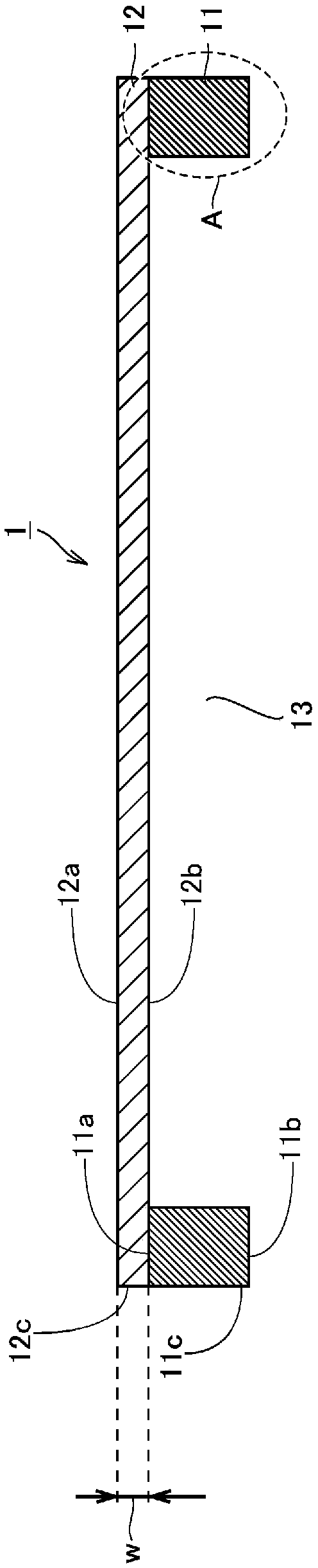
[0080] figure 1 It is a cross-sectional view showing the structure of the compound semiconductor substrate 1 in the first embodiment of the present invention. and also, figure 1 This is a cross-sectional view when cutting is performed on a plane perpendicular to the surface 12 a of the SiC film 12.

[0081] Reference figure 1 The compound semiconductor substrate 1 in this embodiment includes a Si substrate 11 and a SiC film 12.

[0082] The Si substrate 11 has a ring-shaped planar shape. The Si substrate 11 includes a front surface 11a, a back surface 11b, and a side surface 11c. The (111) surface is exposed on the surface 11a of the Si substrate 11. The (100) plane and the (110) plane may be exposed on the surface 11a of the Si substrate 11.

[0083] The SiC film 12 is formed on the surface 11a of the Si substrate 11 (an example of one main surface of the Si substrate). The SiC film 12 includes a surface 12a, a back surface 12b, and a side surface 12c. The back surface 12b of t...

no. 2 approach

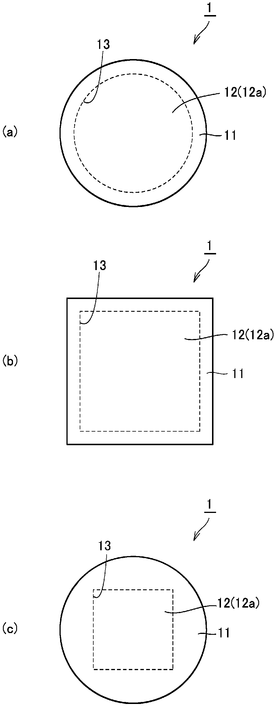
[0114] Figure 16 It is a cross-sectional view showing the structure of the compound semiconductor substrate 1 in the second embodiment of the present invention. and also Figure 16 This is a cross-sectional view when cut in a plane perpendicular to the surface 12 a of the SiC film 12.

[0115] Reference Figure 16 In the compound semiconductor substrate 1 of this embodiment, the SiC film 12 is formed on the outer periphery of the front surface 11a, the side surface 11c, and the back surface 11b of the Si substrate 11. The outer peripheral portions of the front surface 11a, the side surface 11c, and the back surface 11b of the Si substrate 11 are completely covered by the continuous SiC film 12. At the bottom of the recess 13, the back surface 12b of the SiC film 12 is exposed. The thickness of the SiC film 12 decreases at the end of the outer peripheral portion of the back surface 11b. The portion of the SiC film 12 formed on the surface 11a of the Si substrate has a thickness...

no. 3 approach

[0125] Picture 20 It is a cross-sectional view showing the structure of a compound semiconductor substrate 1a in the third embodiment of the present invention. and also, Picture 20 This is a cross-sectional view when cut in a plane perpendicular to the surface 22 a of the GaN film 22.

[0126] Reference Picture 20 The compound semiconductor substrate 1a in this embodiment further includes an AlN film 21 and a GaN film 22.

[0127] The AlN film 21 is formed on the surface 12a of the SiC film 12 (an example of one main surface of the SiC film). The AlN film 21 is a buffer layer for improving the wettability of the SiC film 12 and the GaN film 22. The AlN film 21 has, for example, a thickness of 5 nm or more and 15 nm or less, preferably a thickness of 5 nm or more and 9 nm or less, and more preferably a thickness of 7 nm or more and 9 nm or less.

[0128] The GaN film 22 is formed on the surface 21 a of the AlN film 21. The GaN film 22 has, for example, a thickness of 1500 nm or ...


PUM

PropertyMeasurementUnit
thicknessaaaaaaaaaa
thicknessaaaaaaaaaa
thicknessaaaaaaaaaa

Abstract

Provided are a compound semiconductor substrate, a pellicle film, and a method for manufacturing a compound semiconductor substrate with which it is possible to reduce the film thickness of an SiC film. This method for manufacturing a compound semiconductor substrate is provided with a step for forming an SiC film on the upper surface of an Si substrate, and a step for exposing at least part of the lower surface of the SiC film by wet etching. In the step for exposing at least part of the lower surface of the SiC film, at least the Si substrate and the SiC film are caused to move relative to achemical solution used in the wet etching.

Description

Technical field [0001] The present invention relates to a method of manufacturing a compound semiconductor substrate, a surface film, and a compound semiconductor substrate, and more specifically, to a method of manufacturing a compound semiconductor substrate including a SiC (silicon carbide) film, a surface film, and a compound semiconductor substrate. Background technique [0002] Compared with Si (silicon), SiC is superior in heat resistance and withstand voltage, and has low power loss when used as an electronic device. Therefore, the use of SiC as an epoch-making semiconductor material, for example, high-performance and power-saving inverter devices, power supply components for home appliances, or power semiconductor components for electric vehicles, is advancing. [0003] In addition, SiC has a higher Young's modulus, higher yield strength at high temperatures, and higher chemical stability than Si. Therefore, the use of SiC as MEMS (Micro Electro Mechanical Systems) has bee...

Claims


Application Information

Patent Timeline
Patent Type & Authority Applications(China)
IPC IPC(8): C23C16/42C30B29/36H01L21/306
CPCC30B29/36C23C16/325C30B25/04C30B25/18C30B29/406G03F1/62H01L21/02002H01L21/02381H01L21/02447H01L21/02458H01L21/02488H01L21/02527H01L21/02529H01L21/0254H01L21/0262H01L21/02658H01L21/30604H01L29/0657H01L29/2003H01L29/7786H01L21/02428H01L29/1606B81B2203/0127B81C1/00158C23C16/01C30B33/10C23C16/04C23C16/56H01L21/02167H01L21/02307H01L21/8213H01L21/02164H01L29/1608
Inventor 奥秀彦秀一郎
Owner AIR WATER INC
Why Eureka
Try Eureka