[0027] As mentioned in the background art, the low dropout regulator (LDO) in the prior art has a relatively large static power consumption, which is unacceptable for low power consumption electronic devices that are sensitive to power consumption.
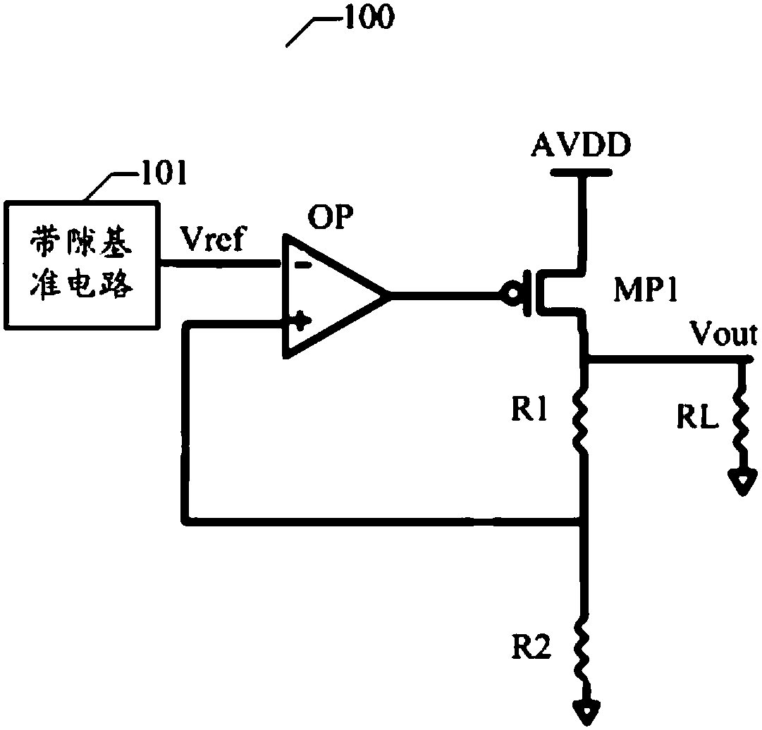
[0028] The inventor of the present application has analyzed the voltage stabilizer in the electronic equipment in the prior art. The mainstream regulators mainly include low dropout regulator (LDO) and diode regulator. Among them, the LDO can be divided into analog LDO and digital LDO.
[0029] First of all, figure 1 It is a schematic diagram of the circuit structure of an analog LDO. See figure 1 , The analog LDO100 is powered by the power supply voltage AVDD, which is suitable for providing the driving voltage Vout to the load RL. The analog LDO 100 may include a bandgap reference circuit 101, an operational amplifier OP, a driving transistor MP1, a first resistor R1, and a second resistor R2, wherein the gate of the driving transistor MP1 is coupled to the output terminal of the operational amplifier OP. When the load current required by the load RL increases/decreases, the feedback voltage (not shown in the figure) fed back to the positive input terminal of the operational amplifier OP after being divided by the first resistor R1 and the second resistor R2 increases/decreases The operational amplifier OP amplifies the voltage difference between the reference voltage Vref generated by the bandgap reference circuit 101 and the feedback voltage to control the increase/decrease of the current output by the driving transistor MP1, while ensuring that the driving voltage Vout is stable In the preset voltage range. The analog LDO100 has a feedback path that can respond to changes in load current, but the bandgap reference circuit 101, the operational amplifier OP, the first resistor R1 and the second resistor R2 will consume quiescent current, making the quiescent power of the analog LDO100 Consumption is greater.
[0030] The digital LDO has a similar circuit structure to the analog LDO100, and may include a feedback path composed of an operational amplifier OP, a counter, multiple weighted PMOS tubes, voltage divider resistors, etc., wherein the multiple weighted PMOS tubes and counters are used to replace the analog LDO100 The drive transistor MP1. When the load current required by the load increases/decreases, the driving current of the driving voltage output by the digital LDO is controlled by controlling the conduction or short-circuit of the plurality of weighted PMOS transistors to meet the current demand of the load. Similarly, a digital LDO also has a feedback path, which can respond to changes in load current, but will also consume quiescent current, making quiescent power consumption larger.
[0031] Secondly, figure 2 It is a circuit diagram of a diode regulator. See figure 2 The diode regulator 200 is powered by the power supply voltage AVDD, and is suitable for providing a driving voltage Vout to the load RL. The three diodes in the figure stabilize the power supply voltage AVDD, where the three diodes are respectively constructed by PMOS transistors MP1, MP2 and MP3. It should be noted that the diode can also be constructed by NMOS transistors. The advantage of the diode regulator 200 is that it does not consume quiescent current. However, due to the feedback path, the size of the diode is fixed. The output drive current cannot also change with the load current of the load RL. Once the load current changes significantly, the output drive voltage Vout will also change accordingly, making the circuit unable to work normally.
[0032] Therefore, the static power consumption of the LDO in the prior art is relatively large, or it cannot meet the requirement that the current drive capability of the regulator changes according to the load current.
[0033] In view of the above-mentioned technical problems, the embodiment of the present invention proposes a voltage stabilizer, which consumes almost no static power consumption when powering electronic equipment, and can also respond to changes in the load current of the load circuit without a feedback path. .
[0034] In order to make the above-mentioned objectives, features and beneficial effects of the present invention more obvious and understandable, specific embodiments of the present invention will be described in detail below in conjunction with the accompanying drawings.
[0035] See image 3 , image 3 As a schematic diagram of the circuit structure of a voltage stabilizer according to an embodiment of the present invention, the voltage stabilizer 300 may include a power input terminal PW, a load output terminal OUT, and a plurality of weight drive circuits connected in parallel, that is, the weight drive circuit in the figure. 101. Weight driving circuit 102... and weight driving circuit 10n. among them:
[0036] The power input terminal PW is configured to be connected to a power supply voltage AVDD, the power supply voltage AVDD comes from a power supply circuit or an instrument, and has a sufficiently large current drive capability.
[0037] The load output terminal OUT is configured to provide a driving voltage Vout to the load circuit 20. Wherein, the load circuit 20 may be a working circuit such as a sensor, a controller, an interface circuit and so on. The load circuit 20 may have different operating modes, for example, may include at least an active mode and a sleep mode. When the load circuit 20 switches between different working modes, the load current consumed by the load circuit 20 is different, and the voltage stabilizer 300 is required to supply it. At the same time, the output of the voltage stabilizer 300 The driving voltage Vout needs to be stable within a preset voltage range. For example, the driving voltage Vout is 1.2V. When the load circuit 20 switches between different working modes, the driving voltage Vout is allowed to vary from 1.08V to 1.32V. This voltage range depends on the The power supply requirements of the load circuit 20 are not particularly limited in this embodiment.
[0038] The input terminals of the multiple weight drive circuits are coupled to the power input terminal PW, the output terminals of the multiple weight drive circuits are coupled to the load output terminal OUT, and the control terminals of the multiple weight drive circuits receive respective The control terminal of the weight driving circuit 101 receives the weight selection signal WS1, the control terminal of the weight driving circuit 102 receives the weight selection signal WS2,..., the control terminal of the weight driving circuit 10n receives the weight selection Signal WSn. The multiple weight driving circuits have different or the same current driving capabilities, which is not limited in this embodiment. The weight selection signal is used to control the weight driving circuit to be turned on or off, that is, the weight selection signal WS1 is used to control the weight driving circuit 101 to turn on or off, and the weight selection signal WS2 is used to control all The weight driving circuit 102 is turned on or off,..., the weight selection signal WSn is used to control the weight driving circuit 10n to turn on or off.
[0039] Wherein, the weight selection signals WS1 to WSn are determined based on the working mode of the load circuit 20. In the following, the description is continued by taking the load circuit 20 having an active mode and a sleep mode as an example. In the active mode, the working circuit in the load circuit 20 consumes a relatively large load current, for example, 300 μA; in the sleep mode, the load current is 2 μA. The magnitude of the load current consumed by the load circuit 20 can be determined through a pre-circuit simulation or parameter design evaluation, which is used as a design basis for setting the weight selection signals WS1 to WSn. In this embodiment, the weight driving circuits have different or the same current driving capabilities. Assuming that the driving capabilities of the respective weight driving circuits are the same, when the load circuit 20 is in the active mode, for example, 300 weight driving circuits can be controlled to be turned on, and when the load circuit 20 is in the sleep mode, 2 can be controlled The weight drive circuit is turned on, and other weight drive circuits are controlled to open. If the driving capabilities of the respective weight driving circuits are different, the load current demand of the load circuit 20 can be satisfied by controlling the conduction or disconnection of different numbers of weight driving circuits.
[0040] Assuming that the driving capability of the power supply voltage AVDD provided by the power input terminal PW is sufficiently large, when the load current consumed by the load circuit 20 increases, the potential of the driving voltage Vout will be lowered, in order to maintain the driving voltage Vout. The potential needs to increase the equivalent driving capability of the weighted driving circuit that is turned on. The equivalent driving capability of multiple weighted driving circuits connected in parallel determines the maximum current drawn from the power input terminal PW. In the same way, when the load current consumed by the load circuit 20 is reduced, the equivalent driving capability of the turn-on weight driving circuit can be reduced. Therefore, in the embodiment of the present invention, since the weight selection signals WS1 to WSn are determined based on the operating mode of the load circuit 20, the load circuit 20 has different requirements for driving current when switching between different operating modes. In some cases, the voltage regulator 300 may switch among different sets of weight selection signals associated with the operating mode of the load circuit 20 to meet the demand of the load circuit 20 for driving current, and provide the load The driving voltage Vout of the circuit 20 is stable within a preset range, which can satisfy the basic function of the voltage stabilizer.
[0041] Furthermore, since the voltage regulator 300 of the embodiment of the present invention does not include a feedback path, the static power consumption of the weight driving circuits 101 to 10n is extremely low, and therefore, figure 1 Compared with the existing technical solutions shown, the solution of the present invention can effectively reduce the static power consumption of the voltage stabilizer, so as to meet the low power consumption application requirements of electronic equipment.
[0042] See Figure 4 , Figure 4 It is a circuit diagram of a voltage stabilizer according to an embodiment of the present invention.
[0043] In a specific implementation, the weight driving circuits 101 to 10n may be MOS transistors, wherein the control terminal of the MOS tube is connected to the weight selection signal, and the input terminal of the MOS tube is coupled to the weight driving circuit. The input terminal, the output terminal of the MOS tube is coupled to the output terminal of the weight driving circuit.
[0044] Furthermore, the weight driving circuits 101 to 10n may be PMOS transistors. The control terminal (that is, the gate) of the PMOS tube MP1 is connected to the weight selection signal WS1, and the control terminal (that is, the gate) of the PMOS tube MP2 is connected to the weight selection signal WS2, ..., The control terminal (that is, the gate) of the PMOS tube MPn is connected to the weight selection signal WSn; the input terminal (that is, the source) of the PMOS tube MP1 is coupled to the input terminal of the weight driving circuit 101, and the The input terminal (that is, the source) of the PMOS transistor MP2 is coupled to the input terminal of the weight drive circuit 102,..., the input terminal (that is, the source) of the PMOS transistor MPn is coupled to the weight drive circuit 10n Input terminal; the output terminal (that is, the drain) of the PMOS tube MP1 is coupled to the output terminal of the weight driving circuit 101, and the output terminal (that is, the drain) of the PMOS tube MP2 is coupled to the weight driving circuit The output terminal of 102,..., the output terminal (that is, the drain) of the PMOS transistor MPn is coupled to the output terminal of the weight driving circuit 10n.
[0045] It should be noted that the weight driving circuits 101 to 10n are not limited to this, and can also be constructed by NMOS transistors.
[0046] It should also be noted that the weight driving circuits in the embodiments of the present invention have different or the same current driving capabilities. Furthermore, when the weight driving circuit is a MOS transistor, the aspect ratios of multiple MOS transistors may be the same or different.
[0047] Preferably, the aspect ratios of the plurality of MOS tubes form a geometric series with a common ratio of 2, that is, the equivalent driving capabilities of the plurality of MOS tubes form a geometric series with a common ratio of 2. More specifically, the aspect ratio of the second MOS tube is twice that of the first MOS tube, the aspect ratio of the third MOS tube is twice that of the second MOS tube, and so on. When controlling the conduction or short-circuit of the multiple MOS transistors, it is equivalent to weighted selection of the equivalent driving capabilities of the multiple MOS transistors, which is easy to implement.
[0048] The embodiment of the present invention also discloses an electronic device. For a schematic structural block diagram, please refer to Figure 5. Figure 5 The illustrated electronic device 400 may include the above image 3 or Figure 4 The voltage regulator 300 is shown.
[0049] In the embodiment of the present invention, the electronic device 400 may further include a control unit 401 configured to generate respective weights of the multiple weight driving circuits 101 to 10n according to the working mode of the load circuit 20 Select signals WS1 to WSn. In a specific implementation, the control unit 401 may be internally integrated or externally coupled to the electronic device 400. Further, the control unit 401 may include control chips such as a single-chip microcomputer, a programmable logic device (Programmable Logic Device, PLD for short), a Field Programmable Gate Array (Field Programmable Gate Array, FPGA for short), etc., and this embodiment does not impose special restrictions. . Preferably, the control unit 401 is a low power consumption control device.
[0050] In a specific implementation, the control unit 401 may include a storage unit 4011 configured to pre-store configuration information for the working mode of the load circuit 20, and the configuration information in each working mode includes at least a set of weights Select the signal. In a specific implementation, the storage unit 4011 may be a storage device of any form. Preferably, the storage unit 4011 may be a low-power storage device.
[0051] Further, the configuration information in each working mode may include multiple sets of weight selection signals, and different sets of weight selection signals correspond to different working conditions of the electronic device 400. For example, the working conditions of the electronic device 400 may include The operating voltage and/or ambient temperature of the electronic device 400 are not limited thereto, and may also include, for example, the ambient humidity and/or luminous flux of the electronic device 400. The control unit 401 is further configured to generate a configuration selection signal (not shown in the figure) according to the working condition, and the configuration selection signal is used to select a group of configuration information from the configuration information of the multiple groups of weight selection signals. That is, the control unit 401 can select one of the multiple sets of weight selection signal configuration information pre-stored in the storage unit 4011 according to the operating conditions of the electronic device 400 and the operating mode of the load circuit 20, respectively. Group configuration information to meet the various load current requirements of the electronic device 400.
[0052] See also Figure 5 with Image 6 , The electronic device 500 of the embodiment of the present invention may further include a sensing unit 402 on the basis of the electronic device 400. The sensing unit 402 is coupled to the control unit 401, and the sensing unit 402 is configured to detect The working conditions of the electronic device 500 are described. Correspondingly, the sensing unit 402 may include one or more of the following sensors: a voltage sensor, a temperature sensor, a humidity sensor, an illumination sensor, and so on.
[0053] Therefore, the electronic device 400 or 500 of the embodiment of the present invention can be weighted by the control unit 401 according to multiple dimensions formed by various factors in the working mode of the load circuit 20 and the working conditions of the electronic device 20 The configuration of the selection signal effectively improves the practicability of the electronic device 400 or 500.
[0054] See Figure 7 , Figure 7 The working waveform diagrams of the load current Iload and the driving voltage Vout corresponding to the four sets of weight selection signals are shown. Wherein, the four sets of weight selection signals respectively correspond to two different working conditions and two different working modes of the electronic device 400 or 500.
[0055] Specifically, when the electronic device 400 or 500 is in working condition 1, if the load circuit 20 is a high current load, the load current Iload is 296.5 μA; if the load circuit 20 is converted to a low current load, the load current Iload is switched to 1.0 μA, at this time, the configuration information of the weight selection signal needs to be switched. It can be seen that the driving voltage Vout after switching is 1.200557V. When the electronic device 400 or 500 is in working condition 2, if the load circuit 20 is a high current load, the load current Iload is 446.0 μA, at this time, the configuration information of the weight selection signal needs to be switched, and the driving voltage Vout after switching is 1.118052V; if the load circuit 20 is converted to a small current load again, the load current Iload is switched to 1.5 μA. At this time, the configuration information of the weight selection signal needs to be switched, and the driving voltage Vout after switching is 1.20256V. It can be seen that when different sets of weight selection signals are switched, the change of the driving voltage can be stabilized within a reasonable voltage range.
[0056] Although the present invention is disclosed as above, the present invention is not limited to this. Any person skilled in the art can make various changes and modifications without departing from the spirit and scope of the present invention. Therefore, the protection scope of the present invention should be subject to the scope defined by the claims.