Wafer surface planarization method

A surface flattening and wafer technology, applied in electrical components, semiconductor/solid-state device manufacturing, circuits, etc., can solve problems such as poor results and inability to completely eliminate wafer surface nanotopography, and achieve easy operation and high efficiency. , the effect of simple process steps

Inactive Publication Date: 2018-11-02
ZING SEMICON CORP
2 Cites 0 Cited by

AI-Extracted Technical Summary

Problems solved by technology

[0010] In view of the prior art described above, the purpose of the present invention is to provide a wafer surface planarization method, which is used to solve t...

Abstract

The invention provides a wafer surface planarization method. The wafer surface planarization method comprises the following steps of 1) providing a wafer, wherein the wafer comprises a first surface and a second surface which are opposite to each other; 2) forming a curing planarization layer on the first surface of the wafer; 3) grinding the second surface of the wafer; 4) grinding the curing planarization layer and the first surface of the wafer to remove the curing planarization layer, and flattening the first surface of the wafer. By the wafer planarization method, surface nanometer morphology of a wafer surface can be thoroughly eliminated, and the wafer planarization method has the advantages of simple process step, relatively high efficiency and the like and is easy to operate.

Application Domain

Semiconductor/solid-state device manufacturing

Technology Topic

Engineering

Image

  • Wafer surface planarization method
  • Wafer surface planarization method
  • Wafer surface planarization method

Examples

  • Experimental program(1)

Example Embodiment

[0046] The following describes the implementation of the present invention through specific specific examples. Those skilled in the art can easily understand other advantages and effects of the present invention from the content disclosed in this specification. The present invention can also be implemented or applied through other different specific embodiments, and various details in this specification can also be modified or changed based on different viewpoints and applications without departing from the spirit of the present invention.
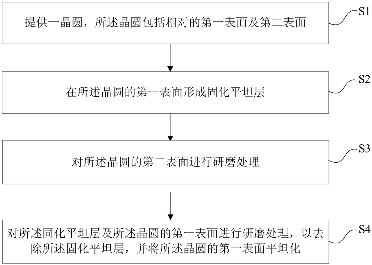
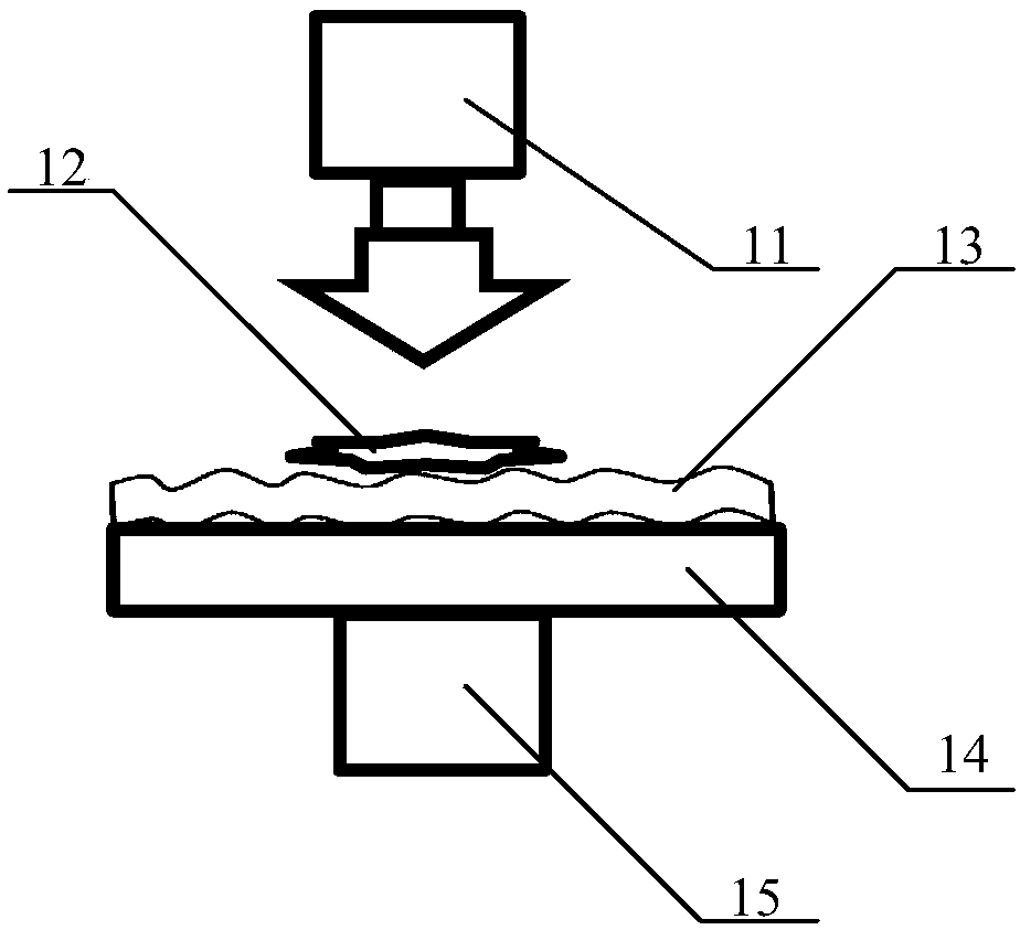
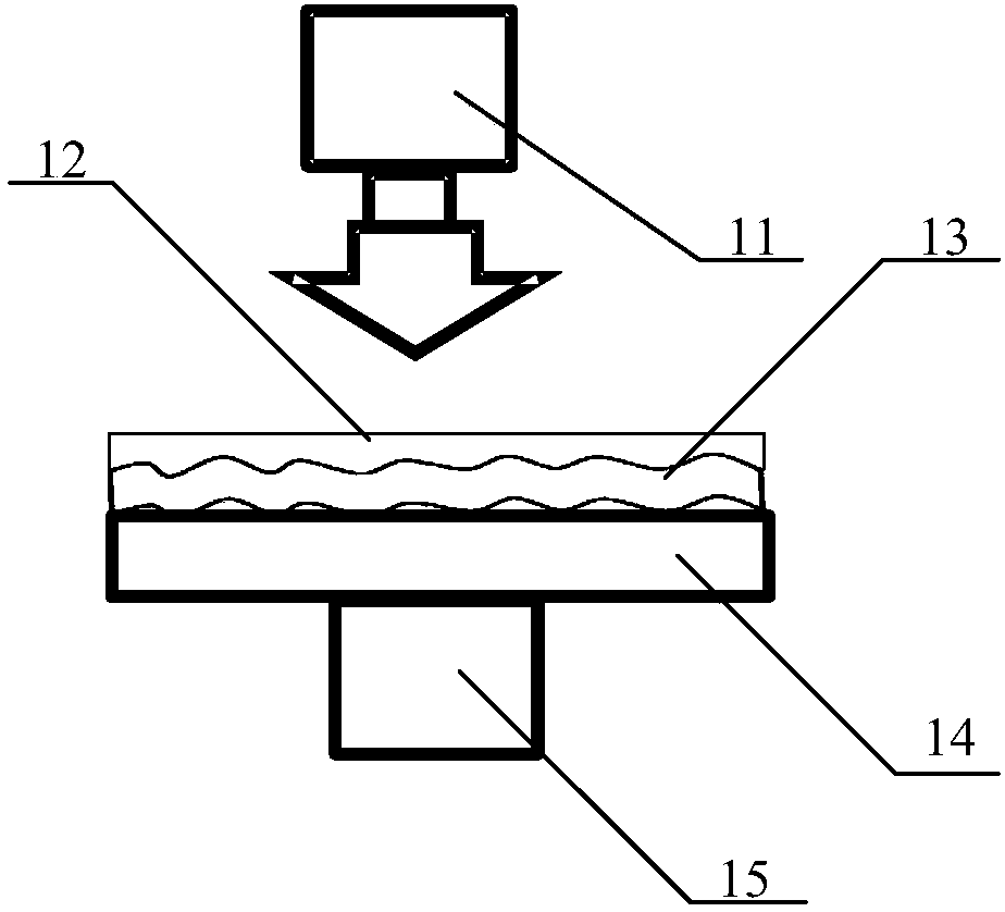
[0047] See Figure 1 to Figure 11. It should be noted that the illustrations provided in this embodiment only illustrate the basic idea of ​​the present invention in a schematic manner, although the illustrations only show the components related to the present invention instead of the actual implementation of the number, shape and For size drawing, the shape, quantity, and proportion of each component can be changed at will during actual implementation, and the component layout type may also be more complicated.
[0048] See figure 1 , The present invention provides a wafer surface planarization method, the wafer surface planarization method includes the following steps:
[0049] 1) Provide a wafer including a first surface and a second surface opposite to each other;
[0050] 2) forming a solidified flat layer on the first surface of the wafer;
[0051] 3) Grinding the second surface of the wafer;
[0052] 4) Grinding the cured flat layer and the first surface of the wafer to remove the cured flat layer and flatten the first surface of the wafer.
[0053] In step 1), please refer to figure 1 In step S1, a wafer 13 is provided. The wafer 13 includes a first surface and a second surface opposite to each other.
[0054] As an example, the wafer 13 is a wafer 13 obtained by wire cutting, and the first surface and the second surface of the wafer 13 are formed with wavy surface nanotopography.
[0055] As an example, step 1) and step 2) further include the step of placing the wafer 13 on a double-end grinder for pretreatment; using a double-end grinder to preprocess the wafer 13 is well known to those skilled in the art , I will not repeat it here.
[0056] In step 2), please refer to figure 1 S2 steps in and Figure 2 to Figure 5 , Forming a solidified flat layer 21 on the first surface of the wafer 13.
[0057] As an example, forming a solidified flat layer 21 on the first surface of the wafer 13 includes the following steps:
[0058] 2-1) Place the wafer 13 on the surface of the vacuum chuck 14, and the second surface of the wafer 13 is in contact with the surface of the vacuum chuck 14; the vacuum chuck 14 sucks the wafer 13;
[0059] 2-2) Drop a liquid curable resin onto the first surface of the wafer 13, such as figure 2 As shown, the vacuum chuck 14 is driven by the drive motor 15 to drive the wafer 13 to rotate to form a resin layer 12 on the first surface of the wafer 13, such as image 3 Shown
[0060] 2-3) The resin layer 12 is planarized; such as Figure 4 As shown, the wafer 13 with the resin layer 12 formed on the surface is first released from the vacuum chuck 14, and then placed on the upper surface of the resin layer 12 using a super-planar structure 16 and pressed firmly The resin layer 12 is used to make the surface of the resin layer 12 as smooth as possible; of course, in other examples, the wafer 13 with the resin layer 12 formed on the surface can also be released from the vacuum chuck 14. Then, the released wafer 13 is transferred to a supporting base, and then a super-planar structure 16 is used to place the upper surface of the resin layer 12, and the resin layer 12 is pressed firmly to make the resin layer The surface of 12 should be as smooth as possible;
[0061] 2-4) curing the resin layer 12 to obtain the cured flat layer 21; specifically, such as Figure 5 As shown, the structure obtained in step 2-2) is placed in a UV chamber 20, and UV (ultraviolet light) irradiation is used to cure the resin layer 12 to obtain the cured flat layer 21.
[0062] As an example, in step 2-2), the speed at which the vacuum chuck 14 drives the wafer 13 to rotate is 500 rpm (revolutions per minute) to 10000 rpm; preferably, in this embodiment, the vacuum chuck 14 drives the wafer 13 The rotation speed of the wafer 13 is 5000 rpm.
[0063] If the first surface of the wafer 13 is not provided with the solidified flat layer 21 and the second surface of the wafer 13 is directly polished later, the wafer 13 can only be temporarily removed during the polishing process. The nano-topography of the second surface, and when the wafer 13 is released after grinding, the nano-topography of the second surface of the wafer 13 will appear again. In the present invention, the cured flat layer 21 is formed on the first surface of the wafer 13, and the cured flat layer 21 has a relatively flat surface. In the subsequent step 3), the second When the surface is polished, the relatively flat solidified flat layer 21 can be used as a reference plane. When the second surface of the wafer 13 is polished, a relatively flat surface can be obtained and the wafer 13 Thorough removal of the nano-topography of the second surface.
[0064] In step 3), please refer to figure 1 S3 steps in and Figure 6 to Figure 8 , The second surface of the wafer 13 is polished.
[0065] As an example, the grinding process on the second surface of the wafer 13 includes the following steps:
[0066] 3-1) Place the structure obtained in step 2) as Image 6 The structure obtained on the vacuum chuck 14 shown in (of course, in other examples, step 2) can be placed on any support plate, such as a grinding plate, etc.), the solidified flat layer 21 and the vacuum The chuck 1 is in contact; the second surface of the wafer 13 is rough-grinded with a 2000-10000 mesh grinding wheel 19; specifically, the grinding wheel 19 is fixed on the rotating shaft 17 via a wheel frame 18, and the grinding wheel 19 is Driven by the rotating shaft 17 to quickly rotate, and rough grinding the second surface of the wafer 13, such as Figure 7 As shown; in this step, the rotation speed of the grinding wheel 19 of 2000 mesh to 10000 mesh can be 50 rpm to 300 rpm, and the grinding time can be set according to actual needs, which is not limited here;
[0067] 3-2) Replace the grinding wheel 19 in step 3-1) with a grinding wheel 19 of 3000 mesh to 50000 mesh, and use the grinding wheel 19 of 3000 mesh to 50000 mesh to finely grind the second surface of the wafer 13, such as Figure 8 As shown; in this step, the rotational speed of the grinding wheel 19 of 3000 mesh to 50000 mesh can be 50 rpm to 300 rpm, and the grinding time can be set according to actual needs, which is not limited here.
[0068] In step 4), please refer to figure 1 S4 steps in and Picture 9 and Picture 11 , Performing grinding treatment on the cured flat layer 21 and the first surface of the wafer 13 to remove the cured flat layer 21 and flatten the first surface of the wafer 13.
[0069] As an example, grinding the solidified flat layer 21 and the first surface of the wafer 13 includes the following steps:
[0070] 4-1) Place the structure obtained in step 3) as Picture 9 The structure obtained on the vacuum chuck 14 shown in (of course, in other examples, step 2) can be placed on any support plate, for example, a grinding plate, etc.), the second surface of the wafer 13 and The vacuum chuck 1 is in contact with each other; the solidified flat layer 21 and the first surface of the wafer 13 are rough-ground with a 2000-10000 mesh grinding wheel 19; specifically, the grinding wheel 19 is fixed to the first surface of the wafer 13 via a wheel frame 18 On the rotating shaft 17, the grinding wheel 19 is rapidly rotated under the drive of the rotating shaft 17, and the solidified flat layer 21 and the first surface of the wafer 13 are rough-ground; the rough grinding in this step Remove the cured flat layer 21, such as Picture 10 As shown; in this step, the rotation speed of the grinding wheel 19 of 2000 mesh to 10000 mesh may be 500 rpm to 10000 rpm, and the rough grinding time may be 1 minute to 10 minutes;
[0071] 4-2) Replace the grinding wheel 19 in step 4-1) with a 3000 mesh to 50000 mesh grinding wheel 19, and use a 3000 mesh to 50000 mesh grinding wheel 19 to finely grind the first surface of the wafer 13, such as Picture 11 As shown; in this step, the rotation speed of the grinding wheel 19 of 3000 mesh to 50000 mesh can be 500 rpm to 10000 rpm, and the fine grinding time can be 1 minute to 10 minutes.
[0072] It should be noted that after step 4), it further includes the steps of sequentially etching and polishing the surface of the wafer 13 obtained in step 4) to further planarize the wafer 13, thereby obtaining a smoother surface The wafer 13. Here, first, either dry etching or wet etching can be used to etch the wafer 13 obtained in step 4) to remove the stress on the wafer 13; then, However, it is not limited to the chemical mechanical polishing process to perform double-side polishing and front-side polishing on the etched wafer 13. The etching and polishing processes are well known to those skilled in the art, and will not be repeated here.
[0073] In summary, the present invention provides a method for flattening the surface of a wafer. The method for flattening the surface of a wafer includes the following steps: 1) Provide a wafer, the wafer including opposite first and second surfaces 2) Form a solidified flat layer on the first surface of the wafer; 3) Grind the second surface of the wafer; 4) Carry out the solidified flat layer and the first surface of the wafer Grinding treatment to remove the solidified flat layer and flatten the first surface of the wafer. The wafer planarization method of the present invention can completely eliminate the surface nano-topography of the wafer surface, and has the advantages of simple process steps, easy operation, and high efficiency.
[0074] The above-mentioned embodiments only exemplarily illustrate the principles and effects of the present invention, but are not used to limit the present invention. Anyone familiar with this technology can modify or change the above-mentioned embodiments without departing from the spirit and scope of the present invention. Therefore, all equivalent modifications or changes made by those with ordinary knowledge in the technical field without departing from the spirit and technical ideas disclosed in the present invention should still be covered by the claims of the present invention.

PUM

no PUM

Description & Claims & Application Information

We can also present the details of the Description, Claims and Application information to help users get a comprehensive understanding of the technical details of the patent, such as background art, summary of invention, brief description of drawings, description of embodiments, and other original content. On the other hand, users can also determine the specific scope of protection of the technology through the list of claims; as well as understand the changes in the life cycle of the technology with the presentation of the patent timeline. Login to view more.

Similar technology patents

Classification and recommendation of technical efficacy words

  • The process steps are simple
  • easy to operate

Preparation method of silver coated copper powder for electronic slurry

InactiveCN102328076ARaw material components are simpleThe process steps are simple
Owner:NINGBO GUANGBO NEW NANOMATERIALS STOCK

Method for preparing ordered coaxial structural micro and nano fibers

InactiveCN102443870AHigh degree of orderly arrangement of fibersThe process steps are simple
Owner:QINGDAO UNIV

Method for extracting and separating components of osmanthus flower or arabian jasmine flower

ActiveCN103695175AAvoid Enzyme BrowningThe process steps are simple
Owner:仙芝科技(福建)股份有限公司 +1

Lancet device

InactiveUS7303573B2inexpensively mass-producedeasy to operate
Owner:ABBOTT DIABETES CARE INC

Rapid and non-invasive optical detection of internal bleeding

InactiveUS20050065436A1easy to operaterapid and accurate result
Owner:HO WINSTON ZONH +2
Why Eureka
Try Eureka