Semiconductor wafer etching system
An etching system and semiconductor technology, which is applied in the manufacture of semiconductor/solid-state devices, discharge tubes, electrical components, etc., can solve the problem of damage to the lower electrode plate, achieve the effects of isolating contact, slowing down the expansion of the gap, and reducing the number
- Summary
- Abstract
- Description
- Claims
- Application Information
AI Technical Summary
Problems solved by technology
Method used
Image


Examples
Embodiment Construction
[0023] In order to make the technical means, creative features, goals and effects achieved by the present invention easy to understand, the present invention will be further described below in conjunction with specific embodiments.
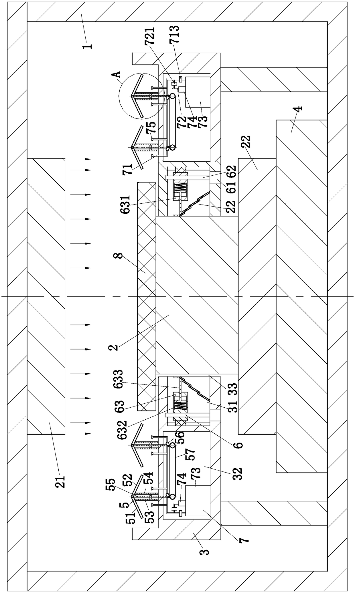
[0024] Such as Figure 1-5 As shown, a semiconductor wafer etching system includes an airtight casing 1, an electrostatic adsorption platform 2, an upper electrode plate 21, a lower electrode plate 22, an annular insulating protection plate 3, an insulating base 4, an ion buffer module 5, and an automatic gap The compensation module 6 and the ion extraction module 7, the inside of the airtight casing 1 is a vacuum environment; the upper electrode plate 21 is located in the center of the top of the airtight casing 1; the insulating base 4 is located at the bottom of the airtight casing 1, The insulating base 4 is used to support the electrostatic adsorption platform 2; the electrostatic adsorption platform 2 is located at the upper end of the insul...
PUM
 Abstract
Description
Claims
Application Information
 - R&D
- Intellectual Property
- Life Sciences
- Materials
- Tech Scout
- Unparalleled Data Quality
- Higher Quality Content
- 60% Fewer Hallucinations
Browse by: Latest US Patents, China's latest patents, Technical Efficacy Thesaurus, Application Domain, Technology Topic, Popular Technical Reports.
© 2025 PatSnap. All rights reserved.Legal|Privacy policy|Modern Slavery Act Transparency Statement|Sitemap|About US| Contact US: help@patsnap.com