Method for preparing oxide thin film transistor by solution method

A technology for oxide thin films and transistors, which is applied in the manufacture of transistors, semiconductor devices, and semiconductor/solid-state devices, etc., can solve the problems of difficult production, fixed components, and high process costs, and achieve the effects of low cost and easy operation.

Inactive Publication Date: 2018-11-06
SOUTH CHINA UNIV OF TECH
View PDF2 Cites 3 Cited by
  • Summary
  • Abstract
  • Description
  • Claims
  • Application Information

AI Technical Summary

Problems solved by technology

However, the vacuum method has the disadvantages of low target utilization and fixed components.
And the process cost is too high, and the large-scale roll-to-roll process is difficult to produce

Method used


Image

  • Method for preparing oxide thin film transistor by solution method
  • Method for preparing oxide thin film transistor by solution method
  • Method for preparing oxide thin film transistor by solution method

Examples


Embodiment 1

[0028] An oxide thin film transistor of this embodiment is prepared by the following method:

[0029] (1) Precursor preparation: 2.576g Zr(NO 3 ) 4 ·5H 2 O (zirconium nitrate pentahydrate) was dissolved in 10ml ethylene glycol monomethyl ether (2-MOE), stirred and aged to obtain a 0.6mol / L insulating layer precursor solution; 0.30083g In(NO 3 ) 3 (indium nitrate) was dissolved in 10ml ethylene glycol monomethyl ether (2-MOE), stirred and aged to obtain a 0.1mol / L active layer precursor solution.

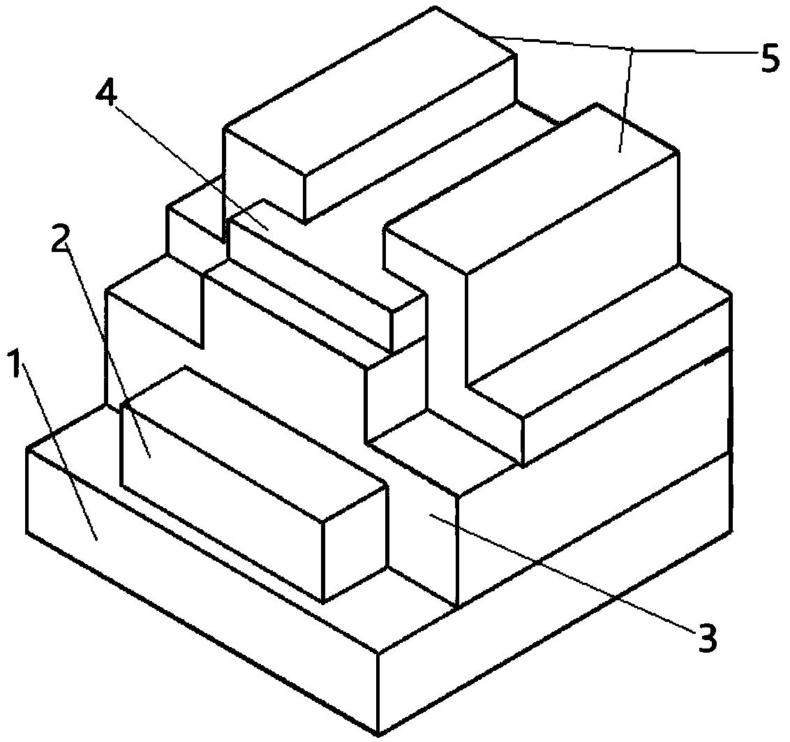
[0030] (2) Substrate preparation: deposit a layer of 150nm ITO electrode on the surface of the glass substrate, wash and dry to obtain the ITO glass substrate.

[0031] (3) Spin-coat the insulating layer precursor solution obtained in step (1) on the ITO glass substrate according to the selected process parameters, the spin-coating speed is 6000rpm, the coating time is 40s each time, and the number of coating times is 3 times. The intermediate annealing temperature is 300° C. fo...

Embodiment 2

[0037] An oxide thin film transistor of this embodiment is prepared by the following method:

[0038] (1) Precursor preparation: 1.288g Zr(NO 3 ) 4 ·5H 2 O (zirconium nitrate pentahydrate) was dissolved in 10ml ethylene glycol monomethyl ether (2-MOE), stirred and aged to obtain a 0.3mol / L insulating layer precursor solution; 0.90249g In(NO 3 ) 3 (indium nitrate) was dissolved in 10ml ethylene glycol monomethyl ether (2-MOE), stirred and aged to obtain a 0.3mol / L active layer precursor solution.

[0039] (2) Substrate preparation: deposit a layer of 150nm ITO electrode on the surface of the glass substrate, wash and dry to obtain the ITO glass substrate.

[0040] (3) Spin-coat the insulating layer precursor solution obtained in step (1) on the ITO glass substrate according to the selected process parameters, the spin-coating speed is 4000rpm, the coating time is 30s each time, and the coating times are 6 times. The intermediate annealing temperature is 300° C. for 5 minut...

Embodiment 3

[0045] An oxide thin film transistor of this embodiment is prepared by the following method:

[0046] (1) Precursor preparation: 2.147g Zr(NO 3 ) 4 ·5H 2O (zirconium nitrate pentahydrate) was dissolved in 10ml ethylene glycol monomethyl ether (2-MOE), stirred and aged to obtain a 0.5mol / L insulating layer precursor solution; 0.60166g In(NO 3 ) 3 (indium nitrate) was dissolved in 10 ml of ethylene glycol monomethyl ether (2-MOE), stirred and aged to obtain a 0.2 mol / L active layer precursor solution.

[0047] (2) Substrate preparation: deposit a layer of 150nm ITO electrode on the surface of the glass substrate, wash and dry to obtain the ITO glass substrate.

[0048] (3) Spin-coat the insulating layer precursor solution obtained in step (1) on the ITO glass substrate according to the selected process parameters, the spin-coating speed is 5000rpm, the coating time is 30s each time, and the number of coating times is 4 times. The intermediate annealing temperature is 300° C...


PUM

PropertyMeasurementUnit
thicknessaaaaaaaaaa
thicknessaaaaaaaaaa

Abstract

The invention belongs to the technical field of thin film transistor preparation and discloses a method for preparing an oxide thin film transistor by a solution method. Zr (NO3)4.5 H2O and In (NO3) 3are dissolved in 2-Methoxyethanol to obtain insulation layer precursor solution and active layer precursor solution respectively. Spin coating of insulation layer precursor solution is performed on ITO glass substrate and annealing is performed to obtain zirconia insulation layer film; spin coating of active layer precursor solution is performed on zirconia insulating layer film and annealing isperformed to obtain indium oxide active layer film; a source/drain electrode is vaporized on the indium oxide active layer to obtain an oxide thin film transistor. The ZrO2 and In2O3 thin film is prepared by preparing an oxide precursor solution, combining with spin coating and annealing technology, the TFT device is prepared by using the two thin films as an insulating layer and an active layer respectively, and the TFT device does not need a vacuum environment, the cost is low, and the operation is simple.

Description

technical field [0001] The invention belongs to the technical field of thin film transistor preparation, and in particular relates to a method for preparing an oxide thin film transistor by a solution method. Background technique [0002] Thin Film Transistor (TFT) is an important switching component in AMLCD and AMOLED pixels. Together with storage capacitors, it forms the drive circuit of the display, thereby realizing large-capacity, high-definition and full-color display of flat-panel displays. Thin-film transistor (TFT), as the core device, directly determines the quality of the display. [0003] In recent years, metal oxide thin film transistors have attracted the attention of researchers because of their excellent performance. At present, most oxide TFTs are prepared by the vacuum method, and the obtained TFTs have excellent electrical properties and the process is relatively mature. However, the vacuum method has disadvantages such as low target utilization rate an...

Claims


Application Information

Patent Timeline
Patent Type & Authority Applications(China)
IPC IPC(8): H01L21/34H01L21/02H01L21/477H01L29/24H01L29/786
CPCH01L21/02422H01L21/02565H01L21/02628H01L21/02664H01L21/477H01L29/24H01L29/66969H01L29/7869
Inventor 宁洪龙周尚雄姚日晖袁炜健史沐杨李志航蔡炜朱镇南魏靖林彭俊彪
Owner SOUTH CHINA UNIV OF TECH
Why Eureka
Try Eureka