

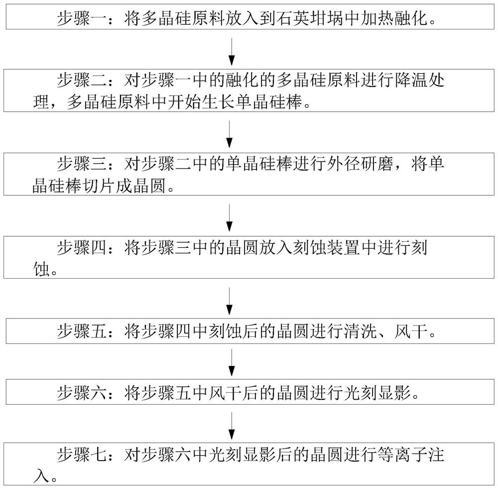
A wafer ion implantation method
A technology of ion implantation and wafer, applied in the direction of electrical components, conveyor objects, transportation and packaging, etc., can solve the problems of limitation, cost waste, and inability to improve the efficiency of etching liquid, so as to improve the clamping degree and reduce impurities Residual amount, effect of improving utilization efficiency
- Summary
- Abstract
- Description
- Claims
- Application Information
AI Technical Summary
Problems solved by technology
Method used
Image

Examples
Embodiment approach
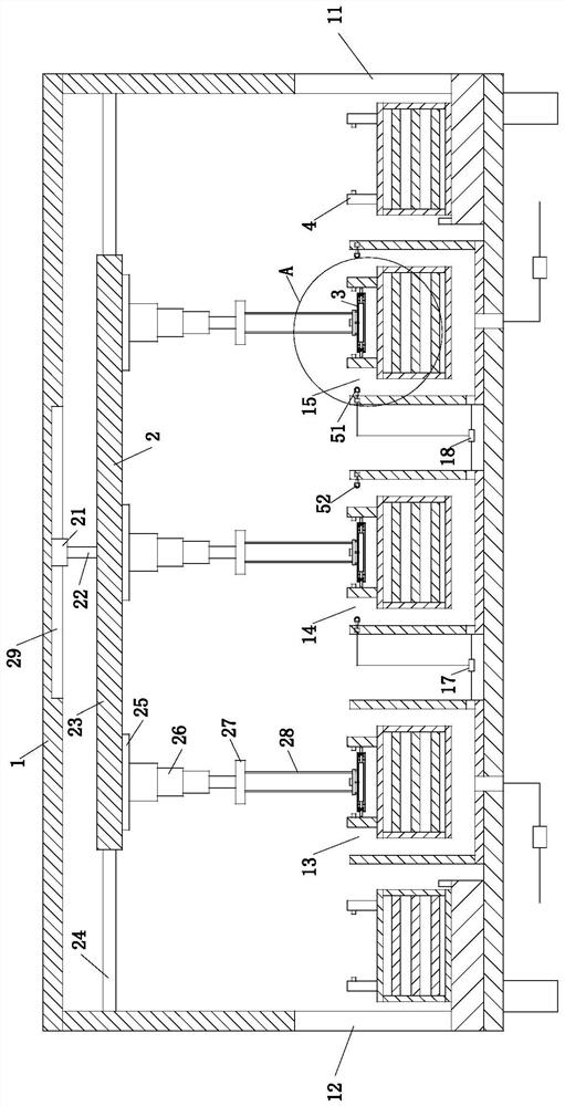
[0046] As an embodiment of the present invention, the mobile module 2 includes a No. 1 slider 21, a fixed rod 22, a fixed plate 23, a sliding telescopic rod 24, a No. 1 mounting seat 25, a multi-stage air pressure rod 26, a mounting plate 27 and Connecting frame 28, No. 1 chute 29 is provided on the top plate inner wall of described reaction chamber 1, and described No. 1 slide block 21 is used for sliding in No. 1 chute 29; Fixedly connected with the No. 1 slider 21; the side surface of the fixed plate 23 is installed on the inner wall of the reaction chamber 1 through the sliding telescopic rod 24; the multi-stage air pressure rod 26 is fixedly installed on the fixed plate 23 through the No. 1 mounting seat 25 The bottom surface of the multi-stage air pressure rod 26 is fixedly connected to the connecting frame 28 through the mounting plate 27; the connecting frame 28 is used for fixedly connecting the grasping module 3. The movement of the No. 1 slider 21 in the No. 1 slide...
PUM
 Abstract
Description
Claims
Application Information