

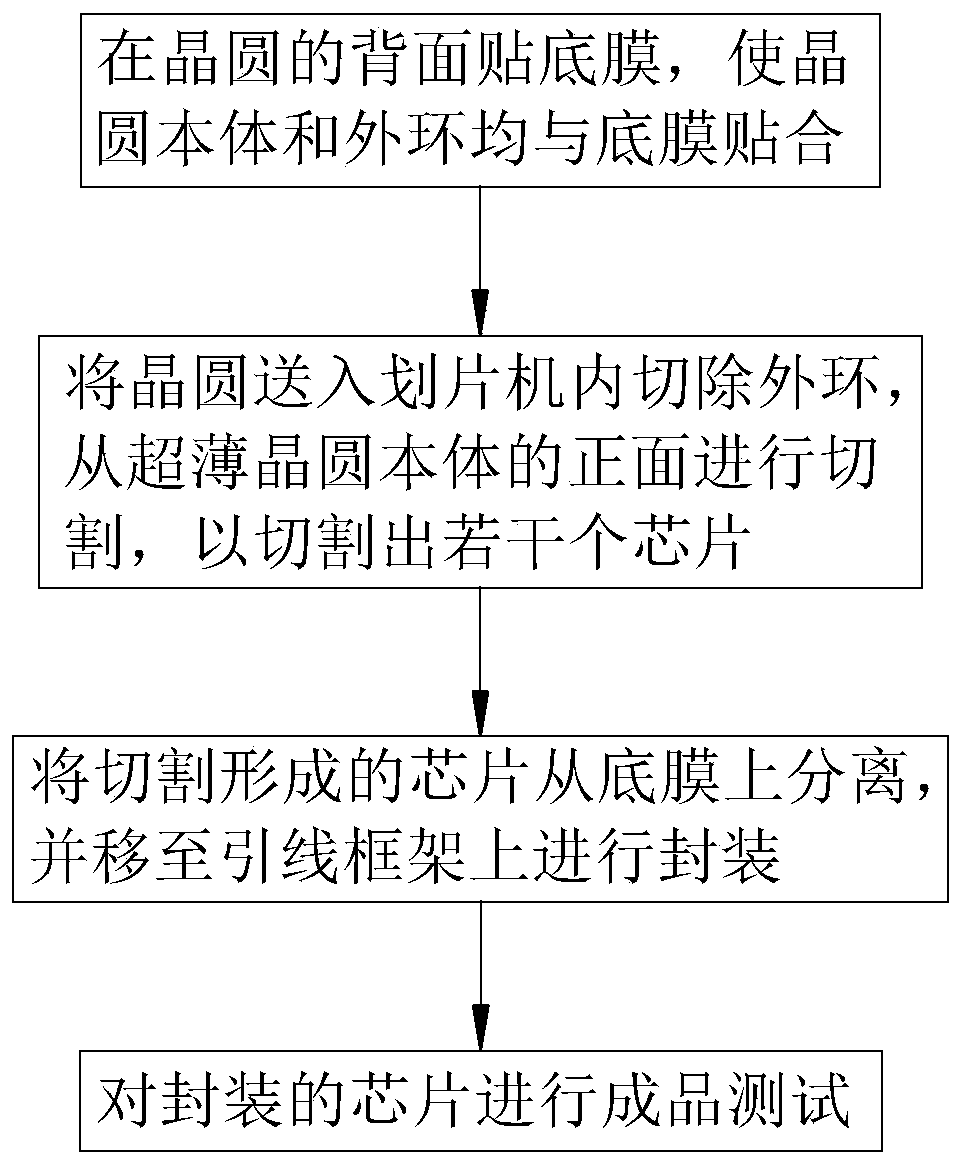
A semiconductor chip production process
A production process and semiconductor technology, applied in the manufacture of semiconductor/solid-state devices, electrical components, circuits, etc., which can solve the problems of weakened adsorption force, inability to adjust the size of adsorption pore size, and clogging of adsorption pores.
- Summary
- Abstract
- Description
- Claims
- Application Information
AI Technical Summary
Problems solved by technology
Method used
Image

Examples
Embodiment approach
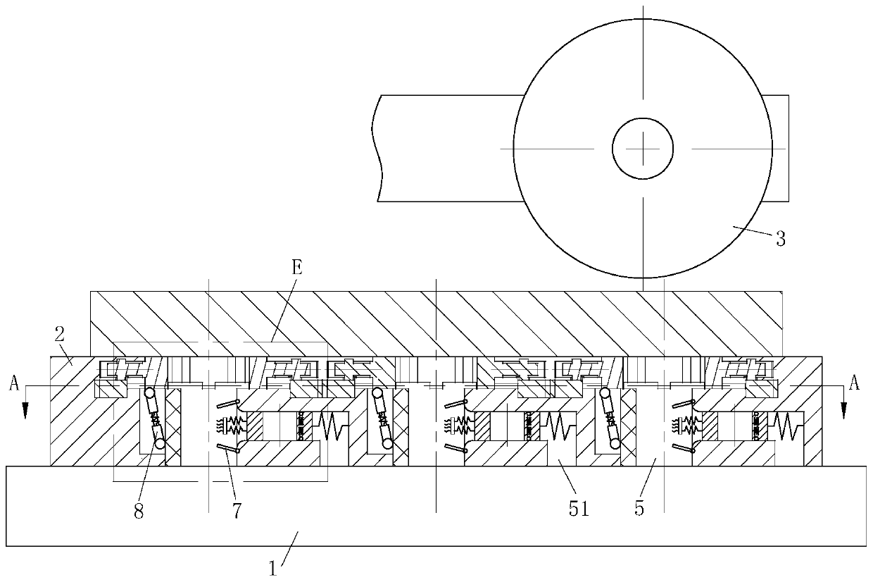
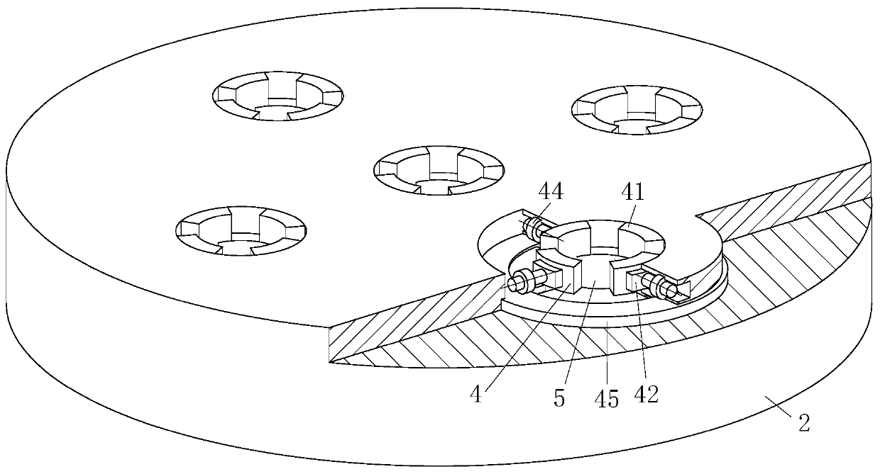
[0039] As an embodiment of the present invention, one side of the adsorption hole 5 is provided with a communication hole 51; one end of the communication hole 51 communicates with the adsorption hole 5; the other end of the communication hole 51 communicates with the outside world; the communication hole 51 A dredging block 52 is slidingly installed inside; the dredging block 52 is provided with a No. 1 through hole 53 in the same direction as the adsorption hole 5 , and the dredging block 52 is used to prevent the adsorption hole 5 from being blocked. When working, after the adsorption hole 5 absorbs the wafer, the communication hole 51 is always connected with the outside world. When the suction hole 5 is vacuumed, the external air pressure pushes the dredging block 52 to move into the adsorption hole 5. After the wafer cutting is completed, the dredging The block 52 returns under the action of the spring, so as to alleviate the blockage of the cutting dust to the adsorption...
PUM
 Abstract
Description
Claims
Application Information