Trench gate device structure having carrier storage region and method for manufacturing the same

A carrier storage and device structure technology, which is applied in semiconductor/solid-state device manufacturing, semiconductor devices, electrical components, etc., can solve the problems of high on-resistance and saturation voltage drop, and low carrier concentration

Pending Publication Date: 2018-11-06
ANHUI PROVINCE QIMEN COUNTY HUANGSHAN ELECTRIC APPLIANCE
View PDF4 Cites 0 Cited by
  • Summary
  • Abstract
  • Description
  • Claims
  • Application Information

AI Technical Summary

Problems solved by technology

[0006] One of the objectives of the present invention is to provide a trench gate device structure with a carrier storage region, which solves the problem that the drift region of the existing device corresponding to the substrate or epitaxial layer described in this patent is close to the second doping described in this patent. The problem of low carrier concentration in the P-region of the region, especially the problem of high on-resistance and saturation voltage drop in the case of low-density cells with a large distance between adjacent trenches

Method used


Image

  • Trench gate device structure having carrier storage region and method for manufacturing the same
  • Trench gate device structure having carrier storage region and method for manufacturing the same
  • Trench gate device structure having carrier storage region and method for manufacturing the same

Examples


Embodiment 1

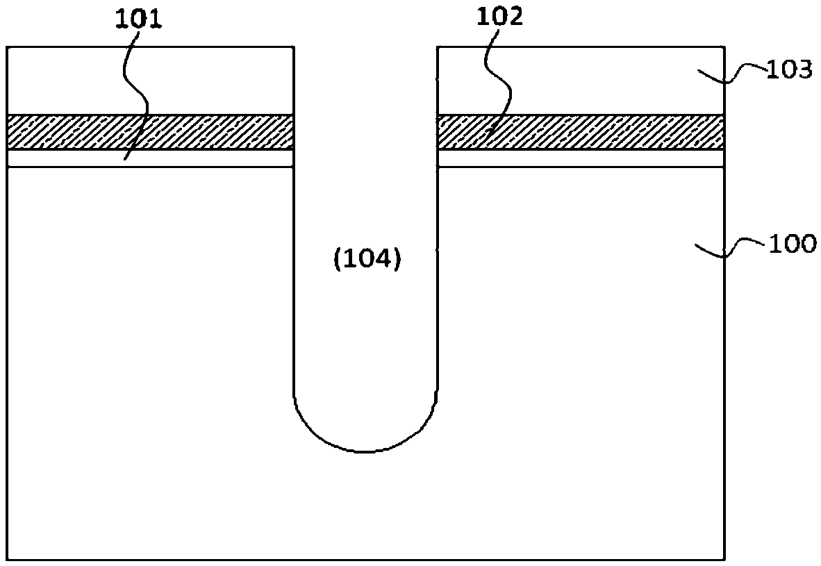
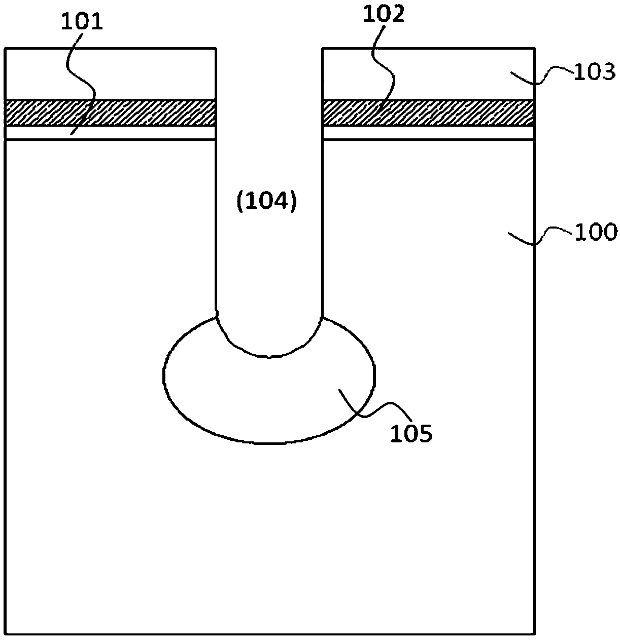
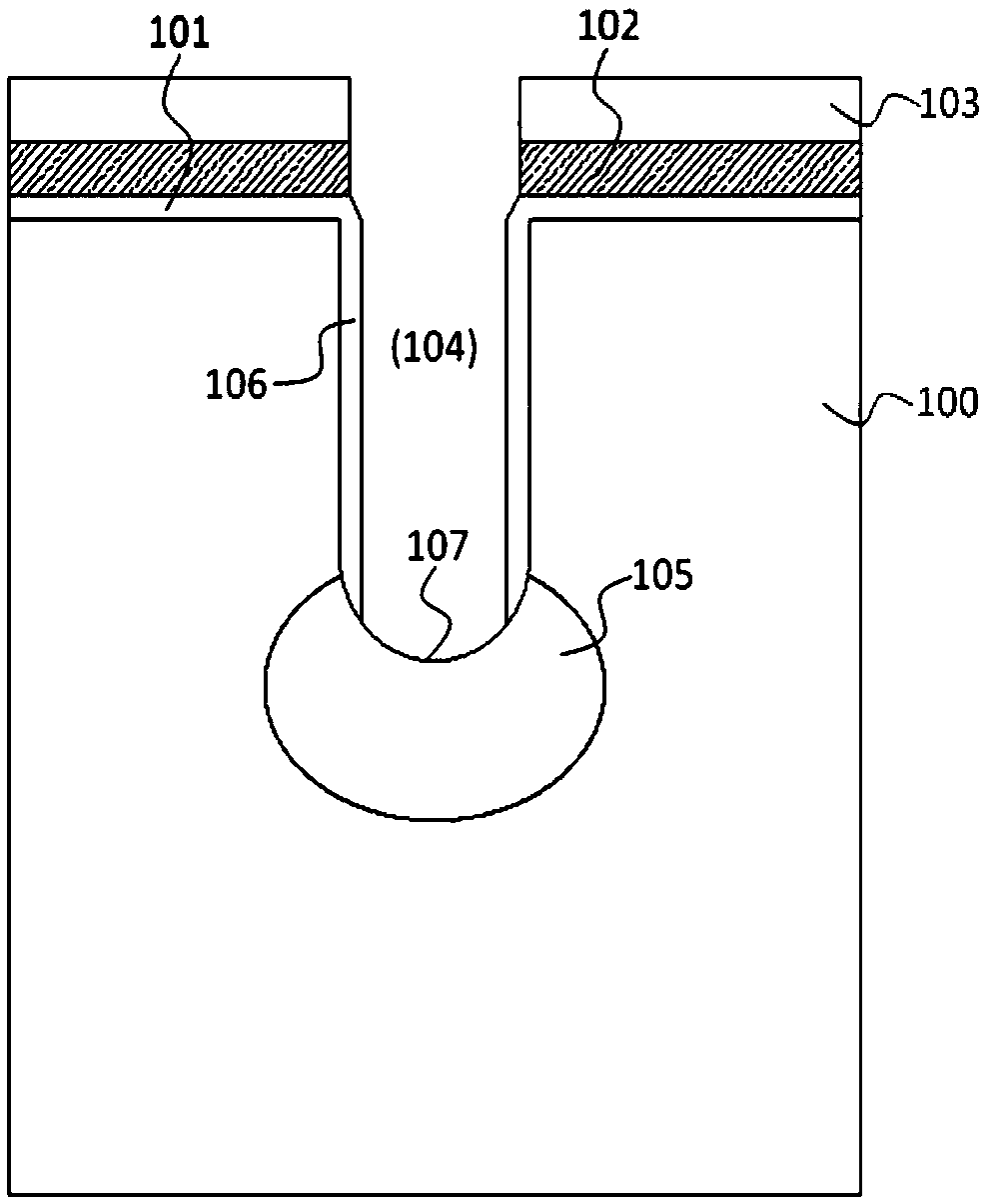
[0045] A trench-gate device structure with a carrier storage region, such as Figure 9 , 10 , 11, including a semiconductor substrate or an epitaxial layer 100, the surface of the semiconductor substrate or the epitaxial layer 100 extends downwards and is provided with a group of trench gates 10, and the trench gate 10 includes an upper trench 104 and an upper trench. For the lower trench 108 below the groove 104, the inner sidewall of the trench gate 10 and the surface of the semiconductor substrate or epitaxial layer 100 are provided with a gate electrode insulating layer 110, and the trench gate 10 is located in the gate electrode insulating layer 110 and filled with Gate electrode 111; the outer side of the trench gate 10 is also provided with a first doped region 105, the first doped region 105 extends laterally and downward from the outer side of the bottom of the upper trench 104, the first doped region 105 Internal doping forms a first-type doped semiconductor that ha...

Embodiment 2

[0056] A trench-gate device structure with a carrier storage region, such as Figure 12 , 13 , 14, including a semiconductor substrate or an epitaxial layer 100, the surface of the semiconductor substrate or the epitaxial layer 100 extends downwards and is provided with a group of trench gates 10, and the trench gate 10 includes an upper trench 104 and a trench located in the upper trench For the lower trench 108 below the groove 104, the inner sidewall of the trench gate 10 and the surface of the semiconductor substrate or epitaxial layer 100 are provided with a gate electrode insulating layer 110, and the trench gate 10 is located in the gate electrode insulating layer 110 and filled with Gate electrode 111 ; a first doped region 105 is also provided outside the trench gate 10 . A fifth doped region 109 is provided below the lower trench 108, and the fifth doped region 109 is doped to form a fifth doped region having the same conductivity type as the semiconductor substrate...

Embodiment 3

[0067] A trench-gate device structure with a carrier storage region, such as Figure 15 , 16 , 17, including a semiconductor substrate or an epitaxial layer 100, the surface of the semiconductor substrate or the epitaxial layer 100 extends downwards and is provided with a group of trench gates 10, and the trench gate 10 includes an upper trench 104 and an upper trench For the lower trench 108 below the groove 104, the inner sidewall of the trench gate 10 and the surface of the semiconductor substrate or epitaxial layer 100 are provided with a gate electrode insulating layer 110, and the trench gate 10 is located in the gate electrode insulating layer 110 and filled with Gate electrode 111 ; a first doped region 105 is also provided outside the trench gate 10 . A sixth doped region 115 is provided below the lower trench 108, and the sixth doped region 115 is doped to form a second type of doped semiconductor having an opposite conductivity type to that of the semiconductor sub...


PUM

PropertyMeasurementUnit
Thicknessaaaaaaaaaa
Thicknessaaaaaaaaaa
Thicknessaaaaaaaaaa

Abstract

The invention discloses a trench gate device structure having a carrier storage region and a method for manufacturing the same. The trench gate device structure comprises a semiconductor substrate oran epitaxial layer, wherein the surface of the semiconductor substrate or the epitaxial layer extends downward and is provided with a group of trench gates; a first doped region is arranged on the outer side of the trench gate; the first doped region is doped to form a first class of doped semiconductors, which have the same conductive type as the semiconductor substrate or the epitaxial layer, have a lateral and longitudinal gradient distribution and have a carrier storage action; such a structure facilitates more carriers to be stored here, thereby reducing on resistance and saturation voltage drop. A method for manufacturing the trench gate device structure is also disclosed, which can improve the processing difficulty and high cost of the existing method. The trench gate device structure having a carrier storage region and the method for manufacturing the same can be widely used in the production and processing field of power devices.

Description

technical field [0001] The invention relates to the field of power devices, in particular to a trench gate device structure with a carrier storage region and a manufacturing method thereof. Background technique [0002] In order to reduce the size of power devices and improve the performance of power devices, trench gate structures are introduced into power devices. Such as Trench Gate Metal Oxide Semiconductor Field Effect Transistor (Trench MOSFET), Trench Insulated Gate Bipolar Transistor (Trench IGBT), Trench Gate MOS Controlled Thyristor (Trench MCT) and similar devices. Trench gate technology introduces devices, compared with planar gate devices, because the resistance of the neck area is eliminated, and the size of the cell composed of the gate and the area between the two gates is greatly reduced, and the current density of the device is increased, so it can be Get lower on-resistance and saturation voltage drop. [0003] However, the reduction of cell size increas...

Claims


Application Information

Patent Timeline
IPC IPC(8): H01L29/06H01L29/36H01L21/265H01L21/225
CPCH01L29/0684H01L29/36H01L21/225H01L21/265
Inventor 饶祖刚王民安项建辉郑科峰
Owner ANHUI PROVINCE QIMEN COUNTY HUANGSHAN ELECTRIC APPLIANCE
Why Eureka
Try Eureka