Programmable gain amplifier circuit based on transconductance feedback unit

A technology of an amplifier circuit and a feedback unit, which is applied in the field of programmable gain amplifier circuits, can solve problems such as larger errors, large chip area consumption, and larger gain errors of programmable gain amplifiers, so as to avoid load effects and reduce chip area. Small, the effect of reducing the gain error

Inactive Publication Date: 2018-11-06
TSINGHUA UNIV
View PDF3 Cites 4 Cited by
  • Summary
  • Abstract
  • Description
  • Claims
  • Application Information

AI Technical Summary

Problems solved by technology

[0004] The existing programmable gain amplifier based on the resistor negative feedback structure requires the resistor R2 to be a relatively small value when the low gain gear is close to 0dB. At this time, the load effect will become obvious, so that the gain expression of The error between R2 / R1 and the actual gain becomes larger, so the load effect will increase the gain error of the programmable gain amplifier; at the same time, the adjustable resistor R2 is realized through a switch resistor array, which requires a large number of resistors, so The switch resistor array consumes a large chip area, and this shortcoming will become more obvious when the integrated circuit manufacturing process continues to improve; in addition, the gain-bandwidth product of the programmable gain amplifier based on the resistor negative feedback structure is a constant, so when When the gain increases, the bandwidth will decrease to the same extent, and the ever-increasing data transmission rate requires the transmitting and receiving system to have a larger bandwidth, so this structure also needs to be further improved in terms of bandwidth

Method used


Image

  • Programmable gain amplifier circuit based on transconductance feedback unit
  • Programmable gain amplifier circuit based on transconductance feedback unit
  • Programmable gain amplifier circuit based on transconductance feedback unit

Examples


Embodiment Construction

[0021] In order to make the object, technical solution and features of the present invention clearer, specific implementation methods will be described in detail below in conjunction with the accompanying drawings.

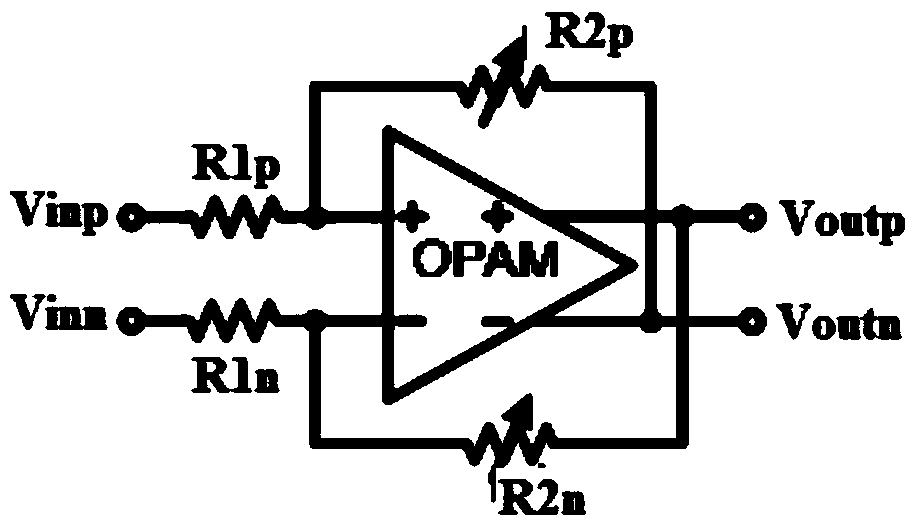
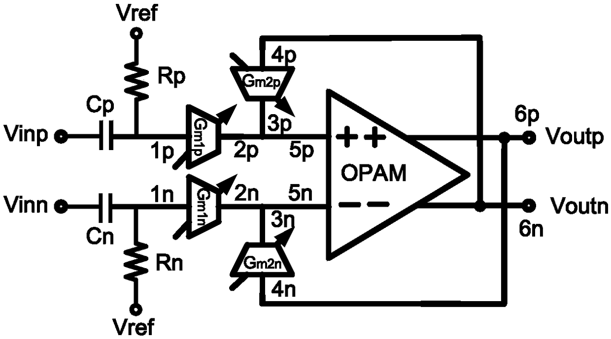
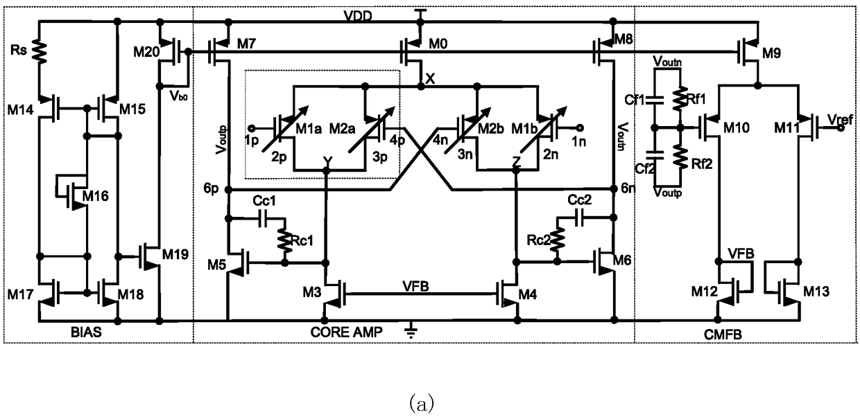
[0022] A kind of programmable gain amplifier circuit based on the transconductance feedback unit proposed by the present invention, its circuit structure is as follows figure 2 As shown, the circuit consists of a positive DC offset suppression circuit, a negative DC offset suppression circuit, a positive transconductance feedback unit, a negative transconductance feedback unit and an operational amplifier OPAM; the operational amplifier OPAM consists of an amplifier circuit, a bias circuit and a common-mode feedback circuit The amplifying circuit is a two-stage Miller amplifier, the bias circuit is a voltage bias circuit proportional to the temperature, and the common-mode feedback circuit is a differential common-mode feedback circuit; the two-stage Miller amplif...


PUM


Abstract

The invention discloses a programmable gain amplifier circuit based on a transconductance feedback unit, and belongs to the design field of analog integrated circuits. The amplifier circuit is composed of a direct current offset suppression circuit, an input transconductance unit, a feedback transconductance unit, and an operational amplifier; the direct current offset suppression circuit is composed of a resistor and a capacitor; the input transconductance unit and the feedback transconductance unit are respectively composed of an MOS transistor array; the operational amplifier is composed ofan amplifying circuit, a bias circuit and a common-mode feedback circuit; the amplifying circuit is a two-stage Miller amplifier; the bias circuit is a voltage bias circuit proportional to temperature; and the common-mode feedback circuit is a differential common-mode feedback circuit. According to the programmable gain amplifier circuit based on the transconductance feedback unit provided by theinvention, the load effect problem in a traditional feedback structure can be effectively solved, and the gain error is reduced; on the premise that the power consumption is not changed, the bandwidth can be greatly improved and the layout area can be reduced, therefore the performance of the programmable gain amplifier can be improved.

Description

technical field [0001] The invention belongs to the field of analog integrated circuit design, in particular to a programmable gain amplifier circuit based on a transconductance feedback unit. Background technique [0002] Since the 21st century, the explosive growth of information technology has made the reception and transmission of signals more and more frequent. For a transmitting and receiving system, the power of the signal received by the receiver is often unpredictable, so in order to avoid desensitization of the system and maximize the dynamic range of the system, it is necessary to add a programmable gain to the receiver Amplifier, so that the receiver can output a fixed power signal. [0003] The gain of the programmable gain amplifier is adjusted by a discrete digital control signal, and has a linear decibel (dB-linear) relationship with the change of the digital control signal. For a programmable gain amplifier, in a large gain range, its gain must have a good...

Claims


Application Information

Patent Timeline
Patent Type & Authority Applications(China)
IPC IPC(8): H03F3/45H03G3/30
CPCH03F3/45376H03G3/30
Inventor 张雷吴伟平
Owner TSINGHUA UNIV
Why Eureka
Try Eureka