CIS (Contact Image Sensor) camera for circuit board and light source module

A light source module and circuit board technology, which is applied in the direction of using optical devices, optical testing for flaws/defects, and material analysis through optical means, which can solve the problem of affecting the judgment ability of circuit boards in taking pictures and affecting the binarization misjudgment of image processing , Take photos with uneven brightness and darkness, etc., to avoid misjudgment, improve consistency, and avoid mutual interference

Pending Publication Date: 2018-11-13
佛山市坦斯盯科技有限公司
View PDF0 Cites 0 Cited by
  • Summary
  • Abstract
  • Description
  • Claims
  • Application Information

AI Technical Summary

Problems solved by technology

Based on the principle of light diffuse reflection, the surface of the circuit board is an incomplete plane, such as figure 1 As shown, due to the existence of diffuse reflection, the camera vertically takes photos to form a light and dark stripes, and the photos taken by the line scan camera and the area array camera all have uneven brightness and darkness. The photo effect is as follows figure 2 As shown, the uneven light and shade of the photo will affect the binarization misjudgment in the image processing, directly affect the software's ability to judge the photo taken by the circuit board, and the phenomenon of inaccurate detection will occur.
When the camera shoots vertically, even with multi-angle light sources, it is still unavoidable to have uneven brightness and darkness. This is because no matter how small the angle between the light source and the vertical direction is, the reflected light is difficult to be parallel to the optical axis of the camera, and the photo taken is still not ideal.

Method used


Image

  • CIS (Contact Image Sensor) camera for circuit board and light source module
  • CIS (Contact Image Sensor) camera for circuit board and light source module
  • CIS (Contact Image Sensor) camera for circuit board and light source module

Examples


Embodiment Construction

[0043] The technical solutions of the present invention will be further described below in conjunction with the accompanying drawings and specific embodiments.

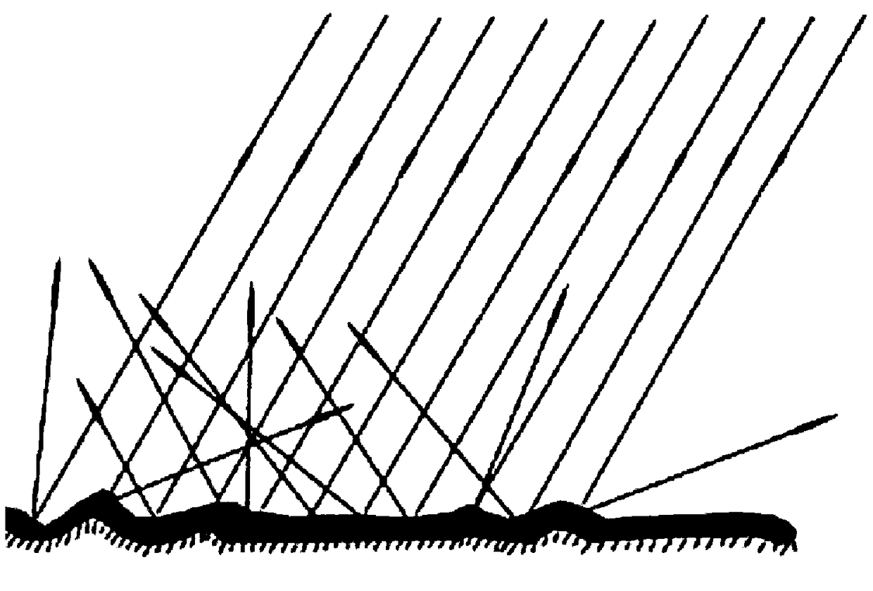
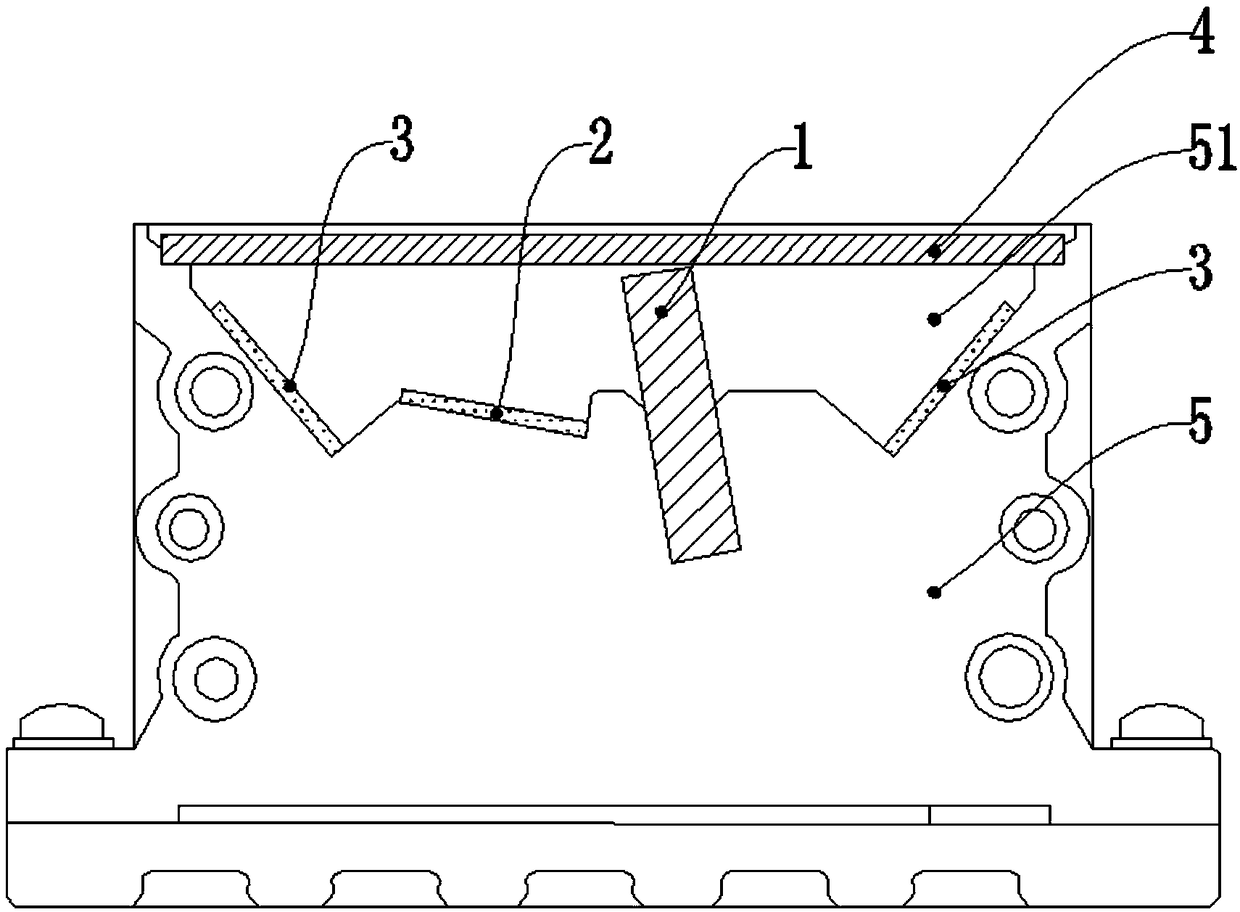
[0044] like Figure 3-6 As shown, a CIS camera and light source module for circuit boards, including a CIS line scan camera 1, a main light source 22 and an auxiliary light source 3, the main light source 22 and the auxiliary light source 3 are linear light sources;

[0045] The main light source 2 and the auxiliary light source 3 are located on the side of the CIS line scan camera 1, and provide light sources for the camera to shoot. There is at least the main light source 2 on one side of the optical axis of the CIS line scan camera 1, and the auxiliary light source 3 on the other side ;

[0046]The light emitting direction of the main light source 2 and the auxiliary light source 3 has the photographed surface 01, the optical axis of the CIS line scan camera 1 is not perpendicular to the photographed surface 01, a...


PUM


Abstract

The invention discloses a CIS (Contact Image Sensor) camera for a circuit board and a light source module. The CIS camera comprises a CIS line-scan digital camera, a main light source and an auxiliarylight source, wherein both the main light source and the auxiliary light source are linear light sources; the main light source and the auxiliary light source are positioned on a side of the CIS line-scan digital camera and are used for providing a light source for camera shooting; the main source is arranged on at least one of both sides of the optical axis of the CIS line-scan digital camera; the auxiliary light source is arranged on the other side of the optical axis of the CIS line-scan digital camera; shot surfaces are arranged on light outgoing directions of the main light source and the auxiliary light source; the optical axis of the CIS line-scan digital camera is not perpendicular to the shot surfaces; main light of both the main light source and the auxiliary light source is notperpendicular to the shot surfaces; and main light of the optical axis of the CIS line-scan digital camera, the main light of the main light source and the main light of the auxiliary light source isintersected on a same straight line of the shot surfaces. The CIS camera is high in application flexibility, low in equipment cost and high in detection precision.

Description

technical field [0001] The invention relates to the technical field of circuit board detection, in particular to a CIS camera and light source module used for circuit boards. Background technique [0002] With the development of electronic technology, the functions of various electronic products are constantly upgraded, and there are higher requirements for the production and testing process of circuit boards. For example, the number of layers of circuit boards is increasing, the internal circuits are becoming denser, the line width and line spacing are smaller, and the detection accuracy is required to be high, etc. [0003] The circuit board inspection device is an advanced online inspection technology. It obtains the image information of the surface of the tested part and compares it with the image information of the qualified part, so as to detect whether the tested part is qualified. Due to the complexity of PCB boards, more and more design circuits, and more and more ...

Claims


Application Information

Patent Timeline
Patent Type & Authority Applications(China)
IPC IPC(8): G01N21/01G01N21/95G01B11/06
CPCG01N21/01G01B11/06G01N21/95
Inventor 门光辉
Owner 佛山市坦斯盯科技有限公司
Why Eureka
Try Eureka