Single-sided light emitting wafer-level chip scale packaging (CSP) structure and preparation method thereof

A wafer-level chip and single-sided light emission technology, which is applied in the manufacture of semiconductor/solid-state devices, electrical components, and electrical solid-state devices, can solve the problems of device reliability and uniformity degradation, poor heat dissipation of light-emitting chips, and increased device costs. , to achieve the effects of improving reliability and uniformity, improving device yield, and high density

Active Publication Date: 2018-11-13
HAIDIKE NANTONG OPTOELECTRONICS TECH CO LTD
View PDF5 Cites 0 Cited by
  • Summary
  • Abstract
  • Description
  • Claims
  • Application Information

AI Technical Summary

Problems solved by technology

Due to the thick phosphor powder or fluorescent colloid layer in such a process, the heat dissipation of the light-emitting chip is poor, and the cost increases; Accuracy requirements
In addition, due to the inconsistent thickness of the phosphor powder passing through the light emitted from the side of the chip and the light emitted from the top surface, it will also cause problems such as impure light output and reduced light efficiency. These problems will increase the cost of the device and greatly reduce the reliability and uniformity of the device.

Method used


Image

  • Single-sided light emitting wafer-level chip scale packaging (CSP) structure and preparation method thereof
  • Single-sided light emitting wafer-level chip scale packaging (CSP) structure and preparation method thereof
  • Single-sided light emitting wafer-level chip scale packaging (CSP) structure and preparation method thereof

Examples


Embodiment

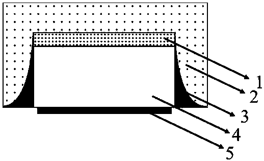
[0048] In this embodiment, the single-sided light-emitting wafer-level chip-level CSP packaging structure, such as figure 1 As shown, a chip 4 and a contact electrode 5 arranged on the chip 4 are included, and a first concentration fluorescent layer 1 is arranged on the light-emitting surface of the chip 4 to form a package A; four sides of the package A are provided with aluminum oxide The reflective wall 3 formed by the aggregation of insulating particles forms a package B; a second concentration fluorescent layer 2 is provided on the top and side surfaces of the package B to form a wafer-level chip-scale packaging structure with light output from one side; the first concentration fluorescent The phosphor concentration in the layer is denoted as w 1 , the phosphor concentration in the second concentration phosphor layer is denoted as w 2 , then w 1 >w 2 ; In this embodiment, the fluorescent layers of the first concentration fluorescent layer 2 and the second concentration f...


PUM

PropertyMeasurementUnit
Thicknessaaaaaaaaaa
Thicknessaaaaaaaaaa
Side wall thicknessaaaaaaaaaa

Abstract

The invention relates to a single-sided light emitting wafer-level chip scale packaging (CSP) structure and a preparation method thereof. The single-sided light emitting wafer-level CSP structure comprises a chip, wherein the light emitting surface of the chip is provided with a first-concentration fluorescent layer so as to form a packaging body A; four side surfaces of the packaging body A are provided with a light reflecting wall formed by the aggregation of insulating particles so as to form a packaging body B; the top surface and side surfaces of the packaging body B are provided a second-concentration fluorescent layer so as to form a single-sided light emitting wafer-level chip scale packaging structure; and the concentration of fluorescent powder in the first-concentration fluorescent layer is recorded as w1, the concentration of fluorescent powder in the second-concentration fluorescent layer is recorded as w2, and the concentration w1 is greater than the concentration w2. Theadvantages lie in that the single-sided light emitting wafer-level CSP structure in the invention introduces side surface light emitting of the chip, the process is relatively simple, the heat dissipation performance of the chip can be improved, the preparation cost of the device can be reduced, and the reliability of uniformity of the device can be improved.

Description

technical field [0001] The invention belongs to the technical field of semiconductor packaging, and in particular relates to a wafer-level chip-level CSP packaging structure and a preparation method thereof. Background technique [0002] Light-emitting diodes (LEDs) have the advantages of small size, long service life, energy saving, environmental protection, fast response, and durability. They are widely used in automotive and indoor lighting, traffic lights, screen displays, and LCD backlights. They are ideal for replacing traditional light sources. light source. The packaging structure of light-emitting diodes usually includes phosphors. The phosphor powder is usually mixed in the encapsulant to change the color of the light emitted by the LED. [0003] Most of the traditional LEDs adopt a formal structure, using silver glue or white glue to fix the chip on the substrate, and connect it to electrical appliances through leads. However, its electrodes and leads will bloc...

Claims


Application Information

Patent Timeline
IPC IPC(8): H01L23/31H01L23/367H01L21/56
CPCH01L21/56H01L23/3114H01L23/3142H01L23/367H01L2224/96
Inventor 杨刚王书昶孙智江
Owner HAIDIKE NANTONG OPTOELECTRONICS TECH CO LTD
Why Eureka
Try Eureka