Packaging structure and method of optical fingerprint chip

A fingerprint chip and packaging structure technology, which is applied in the direction of acquiring/arranging fingerprints/palmprints, radiation control devices, instruments, etc., can solve problems such as high production costs, complex alignment process between optical fingerprint chips and collimators, and reduce The effect of simple production cost and alignment process

Pending Publication Date: 2018-11-13
CHINA WAFER LEVEL CSP
View PDF0 Cites 10 Cited by
  • Summary
  • Abstract
  • Description
  • Claims
  • Application Information

AI Technical Summary

Problems solved by technology

In the existing packaging structure of the optical fingerprint chip, the alignment process between the optical fingerprint chip and the collimator is complicated and the production cost is high

Method used


Image

  • Packaging structure and method of optical fingerprint chip
  • Packaging structure and method of optical fingerprint chip
  • Packaging structure and method of optical fingerprint chip

Examples


Embodiment Construction

[0063] The following will clearly and completely describe the technical solutions in the embodiments of the present invention with reference to the accompanying drawings in the embodiments of the present invention. Obviously, the described embodiments are only some, not all, embodiments of the present invention. Based on the embodiments of the present invention, all other embodiments obtained by persons of ordinary skill in the art without making creative efforts belong to the protection scope of the present invention.

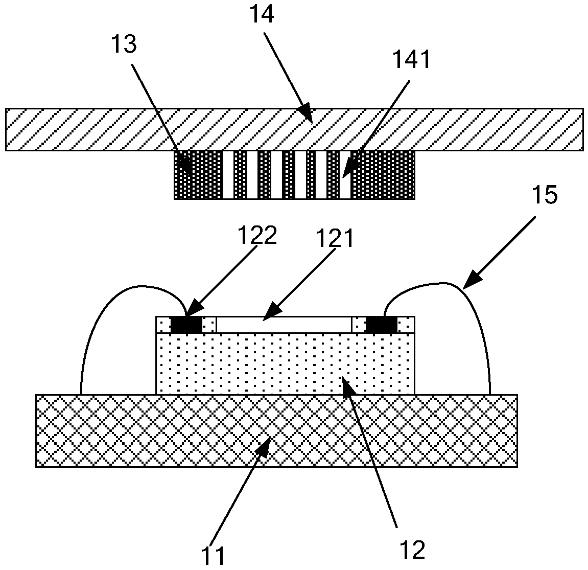
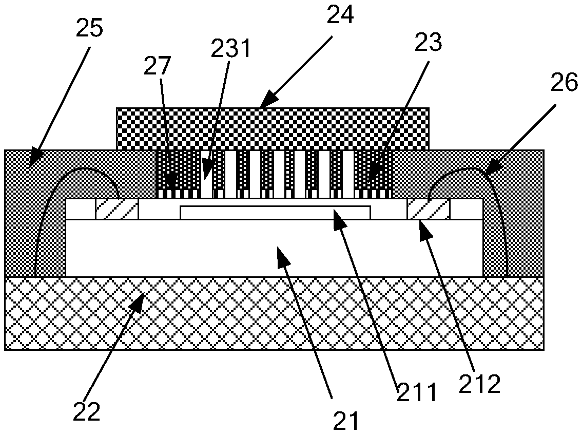
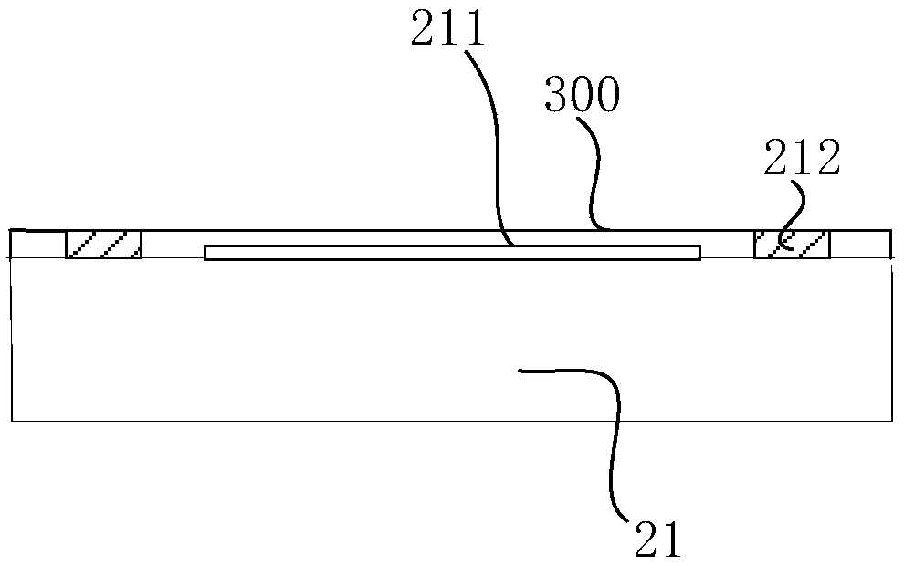
[0064] refer to figure 1 , figure 1 It is a structural schematic diagram of a common packaging structure of an optical fingerprint chip. The packaging structure includes: an optical fingerprint chip 12. The optical fingerprint chip has an opposite front and a back, the back of which is fixed on the surface of the circuit board 11, and the front of which is It has a photosensitive area 121 and welding pads 122 located on both sides of the photosensitive area 1...


PUM


Abstract

The invention discloses a packaging structure and method of an optical fingerprint chip. The packaging structure comprises the optical fingerprint chip and a silicon cover plate; the optical fingerprint chip includes a first surface and a second surface opposite to the first surface, and the first surface comprises light sensitive pixels and bonding pads electrically connected with the light sensitive pixels; the silicon cover plate is attached and fixed to the first surface, and includes through holes arranged opposite to the light sensitive pixels in one to one correspondence; and the lightsensitive pixels of the optical fingerprint chip serve as reference positions of the through holes formed in the silicon cover plate. According to the packaging structure, the silicon cover plate withthe through holes serves as a collimator, the cover plate is fixed onto the optical fingerprint chip and serves as an aligning reference standard, aligning technology is simple, and the manufacturingcost is reduced.

Description

technical field [0001] The invention relates to the technical field of chip packaging, and more specifically, relates to a packaging structure and a packaging method of an optical fingerprint chip. Background technique [0002] With the continuous development of science and technology, more and more electronic devices are widely used in people's daily life and work, which brings great convenience to people's daily life and work, and has become an indispensable and important tool for people today. tool. [0003] At present, the functions of electronic devices are increasingly diversified, and more and more personal information of users is stored. In order to ensure the security of personal information of users, the identification function of electronic devices has become an important function of electronic devices today. Fingerprint identification has many advantages such as uniqueness, high security, and simple operation, and has become the main way for current electronic d...

Claims


Application Information

Patent Timeline
Patent Type & Authority Applications(China)
IPC IPC(8): H01L27/146G06K9/00
CPCH01L27/14618H01L27/14625H01L27/14683H01L27/14687G06V40/1318H01L2224/48091H01L2224/11H01L2924/00014
Inventor 王之奇
Owner CHINA WAFER LEVEL CSP
Why Eureka
Try Eureka