
Pixel structure, OLED (Organic Light-Emitting Diode) display panel comprising pixel structure, and vapor deposition mask

A technology of pixel structure and mask, which is applied in the fields of OLED display and evaporation mask, can solve the problems of narrowing of alignment space, disconnection of connecting bridge, color mixing, etc., and achieve the effect of reducing blurring and improving strength

Pending Publication Date: 2018-11-13
KUNSHAN GO VISIONOX OPTO ELECTRONICS CO LTD
View PDF0 Cites 5 Cited by
  • Summary
  • Abstract
  • Description
  • Claims
  • Application Information

AI Technical Summary

Problems solved by technology

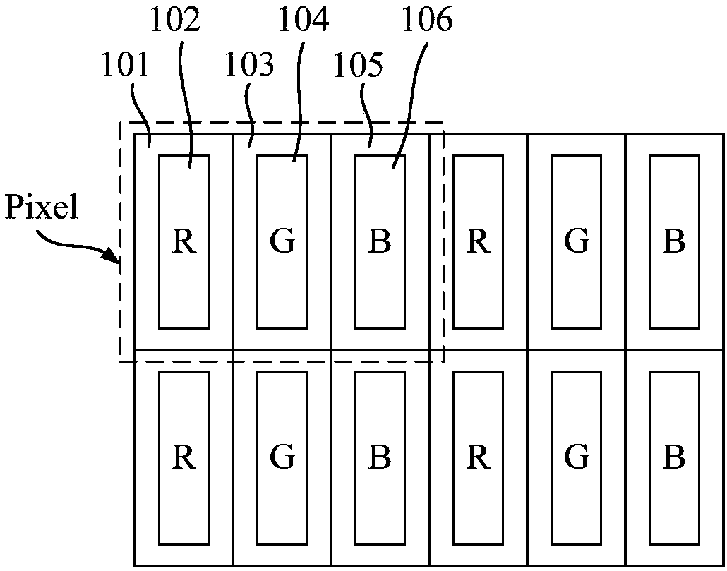
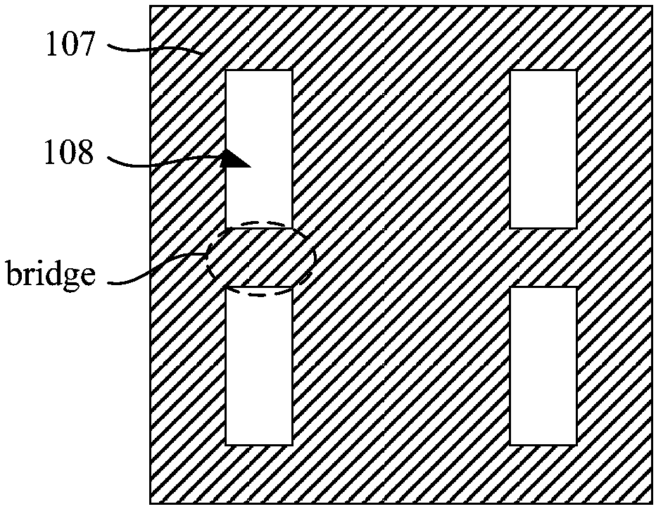
because figure 1 The sub-pixels of the same color in the arrangement mode are arranged up and down in alignment, so the evaporation openings 108 of the FMM must also be arranged in alignment, which makes the connection bridge (bridge) between two vertically adjacent evaporation openings 108 at risk of disconnection
Moreover, the evaporation opening 108 of the FMM needs to correspond to a predetermined pixel position. According to the existing pixel arrangement method, the alignment space between the FMM and the sub-pixel area will be reduced, and defects such as lack of color or color mixing may occur.

Method used


Image

  • Pixel structure, OLED (Organic Light-Emitting Diode) display panel comprising pixel structure, and vapor deposition mask
  • Pixel structure, OLED (Organic Light-Emitting Diode) display panel comprising pixel structure, and vapor deposition mask
  • Pixel structure, OLED (Organic Light-Emitting Diode) display panel comprising pixel structure, and vapor deposition mask

Examples


Embodiment Construction

[0030] As mentioned in the background art, the technical focus of manufacturing a high-PPI OLED display lies in the fine and mechanically stable FMM and the arrangement of pixels. FMM is a key component in the vapor deposition pixel, and problems such as warpage and breakage should be minimized as much as possible to avoid defects that affect the quality of vapor deposition such as smearing and offset of the vapor deposition film layer. The arrangement of pixels and sub-pixels is the main reason for determining whether FMM is prone to warping and fracture. That is, the arrangement of pixels and sub-pixels largely determines the mechanical properties of the FMM, and the mechanical properties of the FMM largely determine the quality of evaporation. Such as figure 2 The FMM shown is to set the evaporation opening corresponding to the position of the sub-pixel of a certain color, because figure 1 The sub-pixels of the same color in the real RGB arrangement method are set up and...


PUM


Abstract

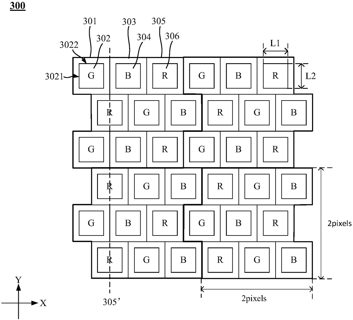
The invention provides a pixel structure, an OLED (Organic Light-Emitting Diode) display screen comprising the pixel structure, and an evaporation mask; the length-width ratio of sub-pixels in the pixel structure is set to be smaller than 1.5:1, which indicates that the shape of the sub-pixel is square or is approximately square, and therefore, maximum apertures can be ensured. Correspondingly, inorder to ensure that the sub-pixel is square or approximately square, four-pixel units (12-sub-pixels ) in the prior art are converted into three pixel units (9 sub-pixels), and the light-emitting areas of the sub-pixels of the same color in adjacent odd-numbered rows and even-numbered rows are staggered; evaporation apertures in the evaporation mask are staggered, and therefore, the strength ofthe evaporation mask can be improved, problems such as the warping and cracking of the evaporation mask can be avoided, and the defects of the spread and shift of the evaporation film layer can be reduced; the shapes and sizes of the first sub-pixel, the second sub-pixel, and the third sub-pixel are identical, and intervals on the evaporation mask are identical, and therefore, the strength of theevaporation mask can be further improved.

Description

technical field [0001] The invention relates to the field of display technology, in particular to a pixel structure, an OLED display containing the pixel structure, and an evaporation mask. Background technique [0002] OLED (Organic Light-Emitting Diode, Organic Light-Emitting Diode) is an active light-emitting device. Compared with the traditional LCD (Liquid Crystal Display, liquid crystal display) display method, the OLED display technology does not require a backlight and has the characteristic of self-luminescence. OLED uses a thin film of organic material and a glass substrate. When an electric current passes through it, the organic material will emit light. Therefore, OLED displays can significantly save power, can be made lighter and thinner, can withstand a wider range of temperature changes than LCD displays, and have a larger viewing angle. OLED display is expected to become the next-generation flat-panel display technology after LCD, and it is one of the most ...

Claims


Application Information

Patent Timeline
IPC IPC(8): H01L27/32H01L51/56C23C14/04C23C14/24
CPCC23C14/044C23C14/24H10K59/353H10K71/00
Inventor 文国哲余珺胡小叙叶訫朱修剑
Owner KUNSHAN GO VISIONOX OPTO ELECTRONICS CO LTD
Learn More