A kind of high-power vertical LED epitaxial structure and its preparation method

A vertical structure and epitaxial structure technology, applied in semiconductor devices, electrical components, nanotechnology, etc., can solve the problems of ohmic contact electrode difficulties, optical and electrical performance limitations, low carrier concentration, etc., to achieve enhanced current expansion, Improving the photoelectric performance and wide application effect

Active Publication Date: 2021-01-22
HEYUAN CHOICORE PHOTOELECTRIC TECH CO LTD
View PDF13 Cites 0 Cited by
  • Summary
  • Abstract
  • Description
  • Claims
  • Application Information

AI Technical Summary

Problems solved by technology

However, the optical and electrical properties of vertical structure LED chips are still limited by the high ohmic contact resistance between metal electrodes and GaN materials, especially the ohmic contact electrodes of p-GaN have a great impact on the performance of LEDs
On the one hand, because the ionization energy of the Mg acceptor element doped in p-GaN is as high as 170meV, the ionization rate of Mg is low, which leads to the low concentration of carriers, and the high doping of p-GaN has not been effective. On the other hand, because there is no metal with a work function larger than p-Ga N (work function is about 6.12eV) in nature, it is difficult to make low-resistance p-GaN ohmic contact electrodes

Method used


Image

  • A kind of high-power vertical LED epitaxial structure and its preparation method
  • A kind of high-power vertical LED epitaxial structure and its preparation method
  • A kind of high-power vertical LED epitaxial structure and its preparation method

Examples


Embodiment 1

[0036] A method for preparing a high-power vertical structure LED epitaxial structure, comprising the following steps:

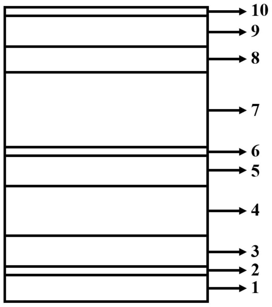
[0037] 1) Place the Si substrate 1 in the MOCVD equipment, select the (111) crystal plane of the Si substrate 1, and sequentially deposit a 2nm pre-coated Al layer 2, a 150nm thick AlN buffer layer 3, and a 500nm thick AlGaN buffer layer 4 , a u-type GaN layer 5 with a thickness of 1000nm;

[0038]Specifically, the operating parameters of the pre-laid Al layer 2: the substrate temperature is 950° C., the reaction chamber pressure is 40 Torr, the graphite disk rotation speed is 900 r / min, and the flow rate of TMAl is 250 sccm;

[0039] The operating parameters for depositing the AlN buffer layer 3: the substrate temperature is 1100° C., the reaction chamber pressure is 50 Torr, the graphite disc rotation speed is 1200 r / min, the flow rate of TMAl is 350 sccm, NH 3 The flow rate is 20slm;

[0040] The operating parameters for depositing the AlGaN buffer laye...

Embodiment 2

[0052] A method for preparing a high-power vertical structure LED epitaxial structure, comprising the following steps:

[0053] 1) Place the Si substrate 1 in the MOCVD equipment, select the (111) crystal plane of the Si substrate 1, and sequentially deposit a 2nm pre-coated Al layer 2, a 150nm thick AlN buffer layer 3, and a 500nm thick AlGaN buffer layer 4 , a u-type GaN layer 5 with a thickness of 1000nm;

[0054] Specifically, the operating parameters of the pre-laid Al layer 2: the substrate temperature is 950° C., the reaction chamber pressure is 40 Torr, the graphite disk rotation speed is 900 r / min, and the TMAl flow rate is 250 sccm;

[0055] The operating parameters for depositing the AlN buffer layer 3: the substrate temperature is 1100° C., the reaction chamber pressure is 50 Torr, the graphite disc rotation speed is 1200 r / min, the flow rate of TMAl is 350 sccm, NH 3 The flow rate is 20slm;

[0056] The operating parameters for depositing the AlGaN buffer layer ...


PUM

PropertyMeasurementUnit
thicknessaaaaaaaaaa
thicknessaaaaaaaaaa
thicknessaaaaaaaaaa

Abstract

The invention discloses a large-power vertical structure LED epitaxial structure. The large-power vertical structure LED epitaxial structure includes a pre-paved Al layer, an AlN buffer layer, an AlGaN buffer layer, a u-type GaN layer, a first graphene layer, an n-type GaN layer, a multi-quantum well, a p-type GaN layer, and a second graphene layer, wherein all the above layers and the multi-quantum well are grown on an Si substrate; and the first graphene layer and the second graphene layer are formed by vapor deposition. The large-power vertical structure LED epitaxial structure has better photoelectric performance and has wide application.

Description

technical field [0001] The invention relates to the field of epitaxial films of photoelectric devices with low-dimensional graphene-enhanced electrical conductivity, in particular to a high-power vertical structure LED epitaxial structure and a preparation method thereof. Background technique [0002] Light-emitting diode (LED) is a semiconductor light-emitting device based on the principle of P-N junction electroluminescence. It has the advantages of high electro-optical conversion efficiency, energy saving, environmental protection, long life, and small size. It is known as the green light source of the 21st century. . LEDs have a wide range of applications and have been used as signal indicators, automotive headlights, LCD backlights, road lighting, indoor lighting, commercial lighting, stadium lighting, medical lighting, and biological lighting. If LEDs can be applied to traditional lighting on a large scale, it will have a very significant energy-saving effect, which i...

Claims


Application Information

Patent Timeline
Patent Type & Authority Patents(China)
IPC IPC(8): H01L33/14H01L33/00B82Y40/00
CPCB82Y40/00H01L33/007H01L33/14
Inventor 李国强
Owner HEYUAN CHOICORE PHOTOELECTRIC TECH CO LTD
Why Eureka
Try Eureka