LED chip and manufacturing method thereof

A technology of LED chips and manufacturing methods, which is applied in the direction of electrical components, circuits, semiconductor devices, etc., can solve the problems of low reliability and easy electrode drop, and achieve the effects of improving reliability, increasing contact area, and improving current expansion performance

Pending Publication Date: 2019-11-22
FOSHAN NATIONSTAR SEMICON
View PDF0 Cites 0 Cited by
  • Summary
  • Abstract
  • Description
  • Claims
  • Application Information

AI Technical Summary

Problems solved by technology

In addition, in the subsequent package bonding, the N electrode 31 is prone to electrode drop, and the reliability is low.

Method used


Image

  • LED chip and manufacturing method thereof
  • LED chip and manufacturing method thereof
  • LED chip and manufacturing method thereof

Examples


Embodiment Construction

[0034] In order to make the object, technical solution and advantages of the present invention clearer, the present invention will be further described in detail below in conjunction with the accompanying drawings.

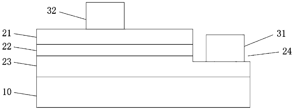
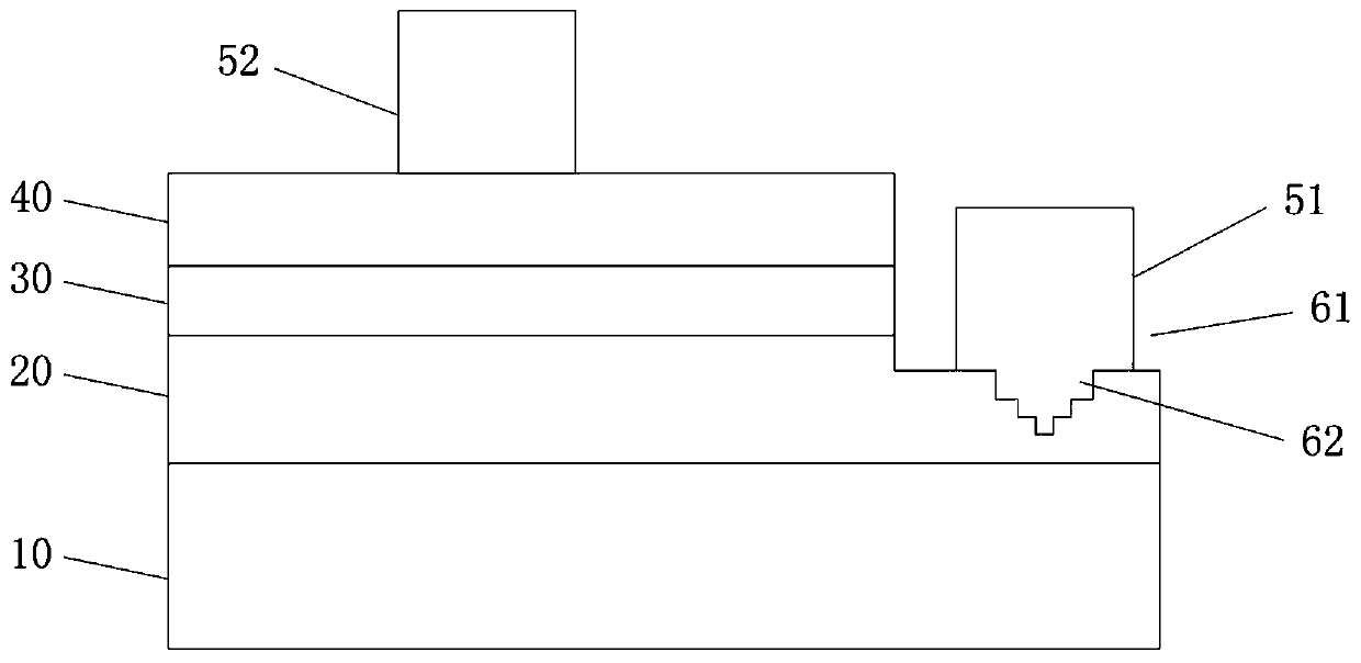
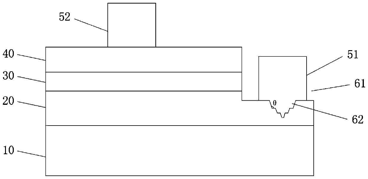
[0035] see figure 2 An LED chip provided by the present invention includes a substrate 10, a first semiconductor layer 20, an active layer 30, a second semiconductor layer 40, a first electrode 51, a second electrode 52, Bare areas 61 and holes 62 .

[0036] The exposed region 61 of the present invention is etched from the second semiconductor layer 40 to the first semiconductor layer 20 to expose the first semiconductor layer 20 . The exposed area 61 is a predetermined area of ​​the first electrode 51 , and the existing first electrode 51 is disposed on the exposed first semiconductor layer 20 .

[0037] There are n holes 62 in the present invention, and n≥2. The n holes 62 are all located in the first semiconductor layer 20 , that is, the holes 62 do not pen...


PUM


Abstract

The invention discloses an LED chip and a manufacturing method thereof. The LED chip includes a substrate, wherein a first semiconductor layer, a active layer, a second semiconductor layer, and a first electrode and a second electrode are sequentially arranged on the substrate; the semiconductor device further comprises an exposed area and n holes, n is larger than or equal to 2, the n holes forma stepped structure, the diameters of the first hole to the nth hole are sequentially decreased progressively, the first electrode is arranged on the exposed first semiconductor layer and extends intothe n holes, and the second electrode is arranged on the second semiconductor layer. According to the invention, the contact area of the first electrode and the first semiconductor layer is increasedthrough the n holes, so that the first electrode and the first semiconductor layer are combined more firmly, the reliability of subsequent packaging and routing is improved, and the current expansioncapability of a chip is improved.

Description

technical field [0001] The invention relates to the technical field of light emitting diodes, in particular to an LED chip and a manufacturing method thereof. Background technique [0002] LED (Light Emitting Diode, Light Emitting Diode) is a semiconductor device that uses carrier recombination to release energy to form light. LED chips have low power consumption, pure chromaticity, long life, small size, fast response time, energy saving and environmental protection, etc. Many advantages. [0003] Light-emitting diodes have now developed into a general-purpose lighting, and the requirements for product characteristics are getting higher and higher. The general requirements are brightness, low voltage, and high reliability. [0004] figure 1 It is a schematic diagram of the structure of an existing LED chip. In an existing LED chip, the epitaxial layer is generally etched to the N-type GaN layer 23 to form an exposed region 24, and then formed on the exposed N-type GaN la...

Claims


Application Information

Patent Timeline
Patent Type & Authority Applications(China)
IPC IPC(8): H01L33/38
CPCH01L33/382H01L2933/0016
Inventor 崔永进王硕张状庄家铭
Owner FOSHAN NATIONSTAR SEMICON
Why Eureka
Try Eureka