Printed circuit board manufacturing method and printed circuit board
A technology of printed circuit boards and manufacturing methods, which is applied in the fields of printed circuit manufacturing, printed circuits, printed circuits, etc., can solve problems such as printed circuit board bursting, improve product reliability, alleviate mechanical impact, and protect from damage Effect
- Summary
- Abstract
- Description
- Claims
- Application Information
AI Technical Summary
Problems solved by technology
Method used
Image
Examples
Embodiment 1
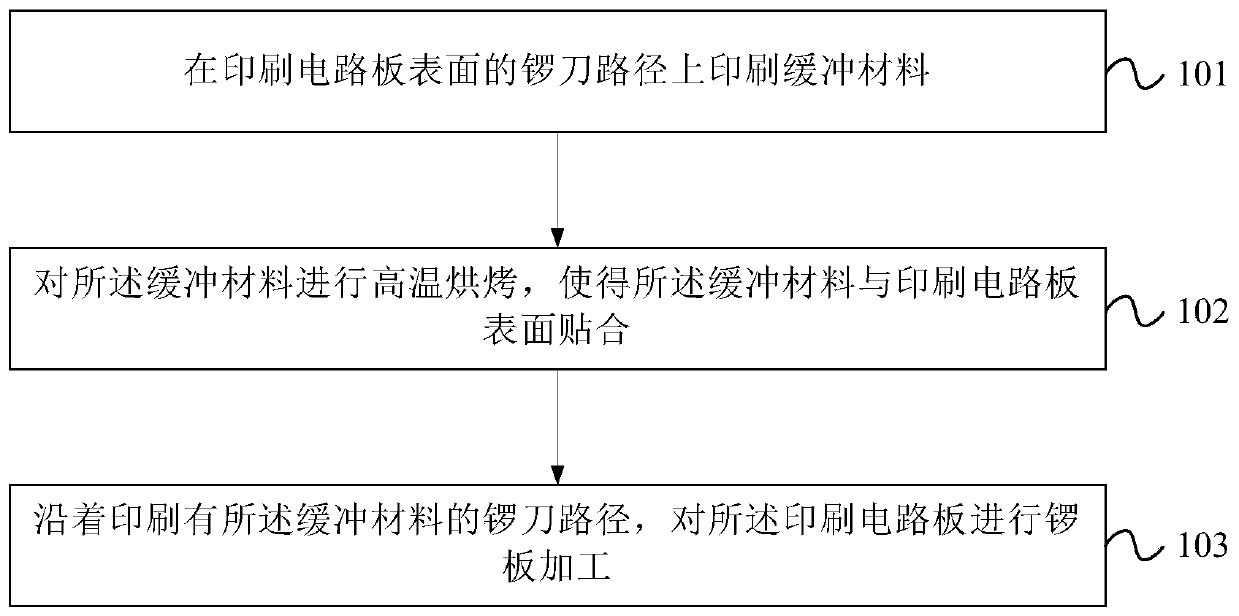
[0059] The first embodiment of the present invention provides a manufacturing method of a printed circuit board. figure 1 It is a flowchart of a method for manufacturing a printed circuit board according to the first embodiment of the present invention. Such as figure 1 As shown, the method in this embodiment may include:
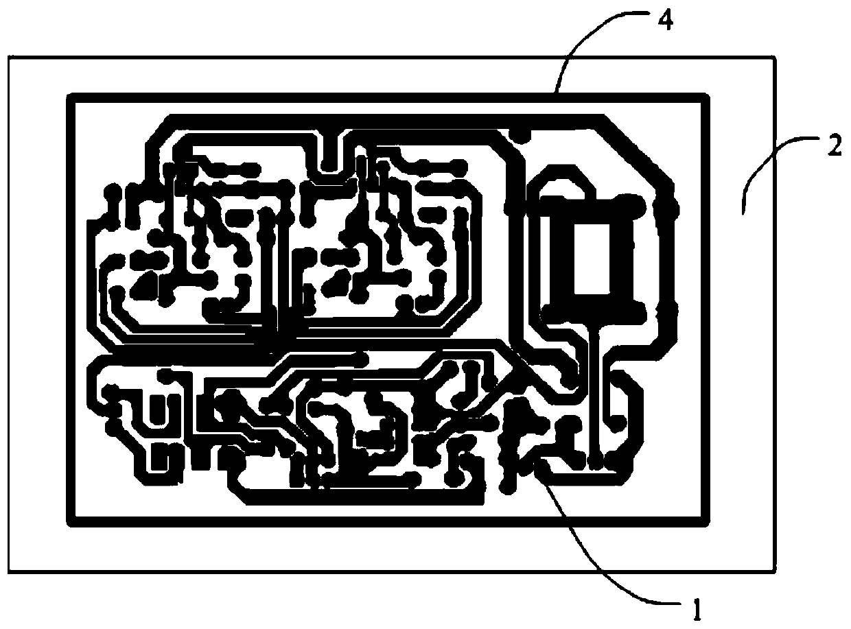
[0060] Step 101: Print a buffer material 4 on the gong knife path 3 on the surface of the printed circuit board.
[0061] Wherein, the gong knife path 3 may be a cutting path of the gong knife during subsequent processing of the gong knife on the printed circuit board. On the surface of the printed circuit board, a layer of buffer material 4 can be printed corresponding to the path 3 of the knife. The buffer material 4 can be a material capable of buffering, such as a buffer film or solder mask ink.
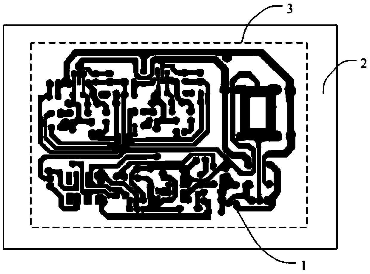
[0062] figure 2 It is a schematic diagram of the path 3 of the gong knife in the method for manufacturing a printed circuit board according to the first embodiment...
Embodiment 2
[0073] The second embodiment of the present invention provides a manufacturing method of a printed circuit board. In this embodiment, on the basis of the technical solution provided in the first embodiment, the solder resist ink is used as the buffer material.
[0074] Figure 4 It is a flow chart of the manufacturing method of the printed circuit board provided by the second embodiment of the present invention. Such as Figure 4 As shown, the method in this embodiment may include:
[0075] Step 201: Print a solder mask ink on the surface of the printed circuit board.
[0076] Step 202: Determine the gong knife path of the printed circuit board, and perform film alignment on the printed circuit board according to the gong knife path of the printed circuit board.
[0077] Step 203: Perform exposure and development operations on the printed circuit board so that the distribution of the solder mask ink is consistent with the path of the knife.
[0078] In this embodiment, steps 201 to 20...
Embodiment 3
[0088] The third embodiment of the present invention provides a method for manufacturing a printed circuit board. In this embodiment, on the basis of the technical solution provided in the first embodiment, the buffer material is intermittently arranged on the path of the gong knife.
[0089] Figure 5 This is a flowchart of a method for manufacturing a printed circuit board provided in the third embodiment of the present invention. Such as Figure 5 As shown, the method in this embodiment may include:
[0090] Step 301: Determine the gong knife path 3 of the printed circuit board.
[0091] Step 302: Print a section of buffer material 4 on the path 3 of the gong knife every predetermined distance.
[0092] In this embodiment, the buffer material 4 can be printed on the gong knife path 3 on the surface of the printed circuit board through steps 301 to 302.
[0093] The method for determining the path 3 of the gong knife belongs to the prior art and will not be repeated here. After the...
PUM
 Abstract
Description
Claims
Application Information


