
Integrated circuit layout checking method

An inspection method and integrated circuit technology, applied in electrical digital data processing, special data processing applications, instruments, etc., can solve the problems of inability to locate through-hole density, insufficient inspection, and high software cost, so as to improve inspection efficiency and inspection coverage. Full, easy-to-change effects

Pending Publication Date: 2018-11-16
SHANGHAI HUALI MICROELECTRONICS CORP
View PDF8 Cites 1 Cited by
  • Summary
  • Abstract
  • Description
  • Claims
  • Application Information

AI Technical Summary

Problems solved by technology

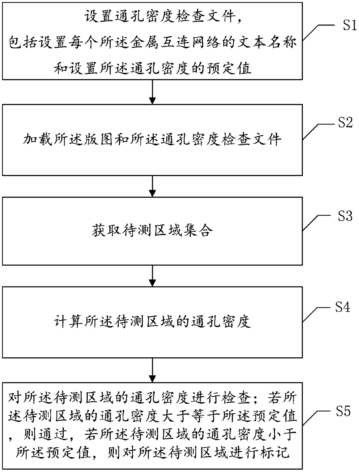
[0004] The purpose of the present invention is to provide an inspection method of integrated circuit layout to solve the problems of heavy workload and insufficient inspection in existing inspection methods
[0005] Another object of the present invention is to provide a method for inspecting the layout of an integrated circuit to solve the problem that the existing inspection method cannot accurately locate the area with insufficient through-hole density and the cost of using software is high

Method used


Image

  • Integrated circuit layout checking method
  • Integrated circuit layout checking method
  • Integrated circuit layout checking method

Examples


Embodiment Construction

[0032] The specific implementation manner of the present invention will be described in more detail below with reference to schematic diagrams. The advantages and features of the present invention will be more apparent from the following description. It should be noted that all the drawings are in a very simplified form and use imprecise scales, and are only used to facilitate and clearly assist the purpose of illustrating the embodiments of the present invention.

[0033] As mentioned in the background art, in the layout design of integrated circuits, it is hoped that the metal connection area can have enough through holes, and the current inspection methods for the through hole density of the metal connection area include manual inspection methods and the use of automated tools to calculate the voltage drop method, the former has a large workload and the integrity of the inspection is limited, and the latter cannot accurately locate the area with insufficient via density, an...


PUM


Abstract

The invention provides an integrated circuit layout checking method. The integrated circuit layout checking method comprises the steps that a through hole density checking file is arranged; a to-be-detected area set is obtained; the through hole density of to-be-detected areas is calculated; the through hole density of to-be-detected areas is checked; if the through hole density of to-be-detectedareas is greater than or equal to a predetermined value, if yes, the through hole density of to-be-detected areas is smaller than the predetermined value, the to-be-detected areas are marked. According to the method, through hole density checking is converted into special layout design rule checking, automatic checking of the through hole density is achieved through design rule checking files, accurate positioning of missed through holes can be achieved, a checking coverage range is wide, prompt marking can be quickly and efficiently conducted on the areas which do not comfort to design rules,layout change of layout designers is facilitated, the checking efficiency is improved, and the cost is saved.

Description

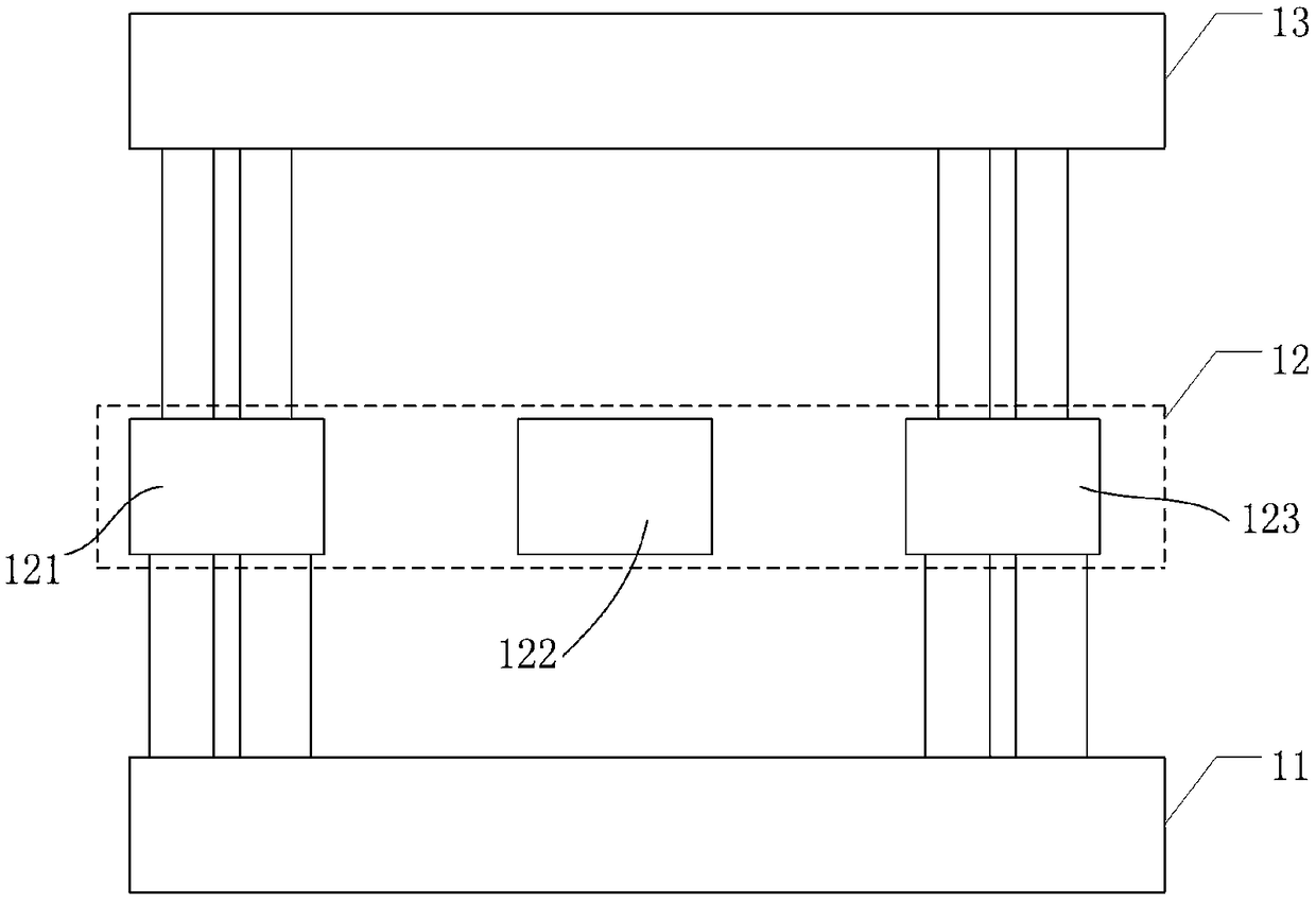
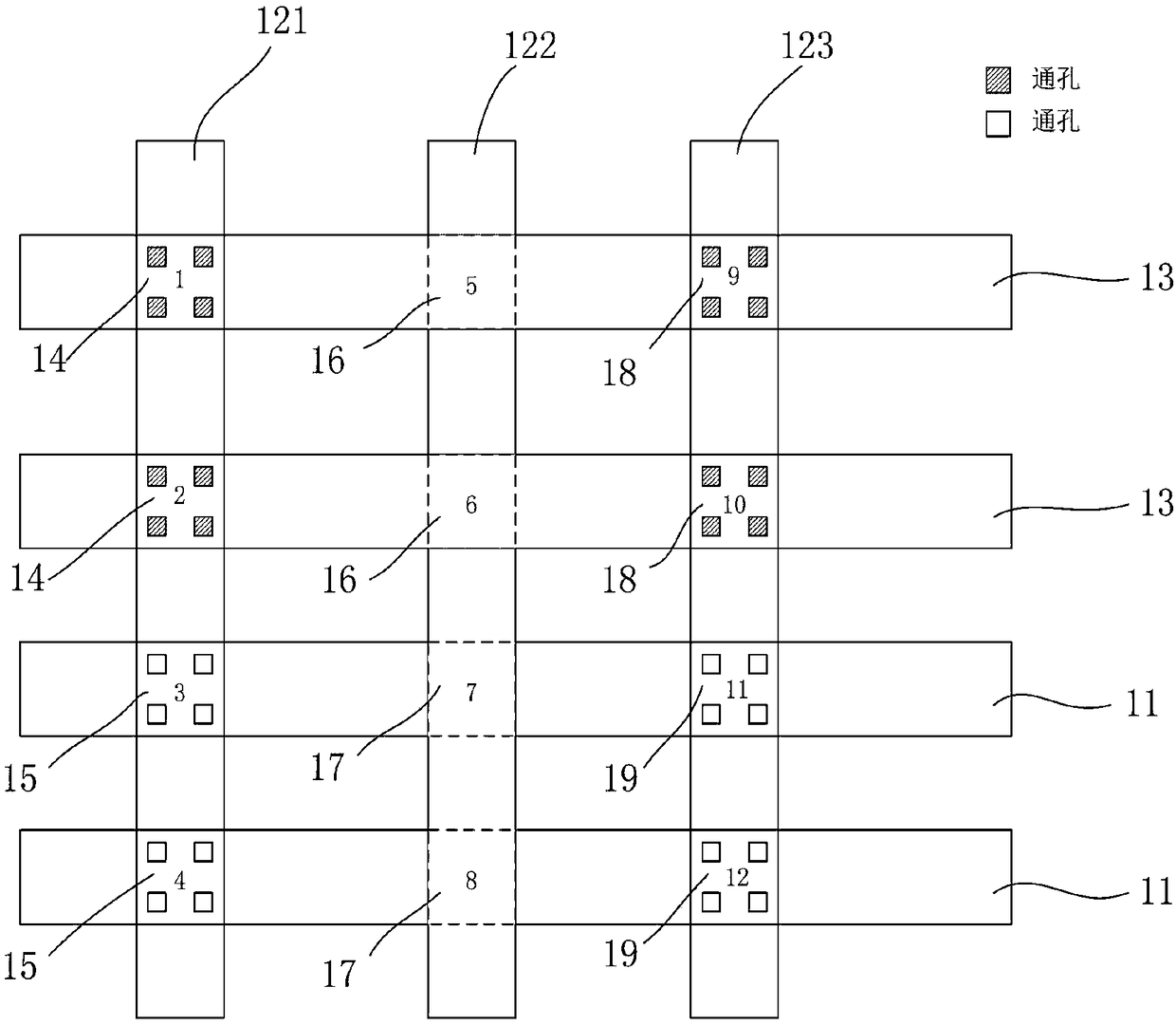
technical field [0001] The invention relates to the field of semiconductor manufacturing, in particular to a method for inspecting an integrated circuit layout. Background technique [0002] In the back-end process of semiconductor device manufacturing, a multi-layer metal interconnection layer consisting of metal interconnection lines and insulating layers will be grown on the semiconductor substrate, and then through holes will be made in the insulating layer, and metals will be deposited in the through holes to achieve different Connections between layer metal traces. The number of vias between metal connections of different layers will affect the circuit performance, too small a number will make the resistance voltage drop too large, so it is generally hoped that there are enough vias in the connection area during layout design. [0003] At present, there are two methods for checking the through-hole density in the connection area. One is manual inspection, which has a ...

Claims


Application Information

Patent Timeline
IPC IPC(8): G06F17/50
CPCG06F30/392G06F30/398
Inventor 陈颖颖杨婷李浩然
Owner SHANGHAI HUALI MICROELECTRONICS CORP
Learn More