
3D memory word line connecting zone making method and 3D memory

A memory and connection area technology, applied in the direction of electric solid-state devices, semiconductor devices, electrical components, etc., can solve the problem of contact deviation and other problems, achieve the effect of easy control, small size, and avoid etching punch-through

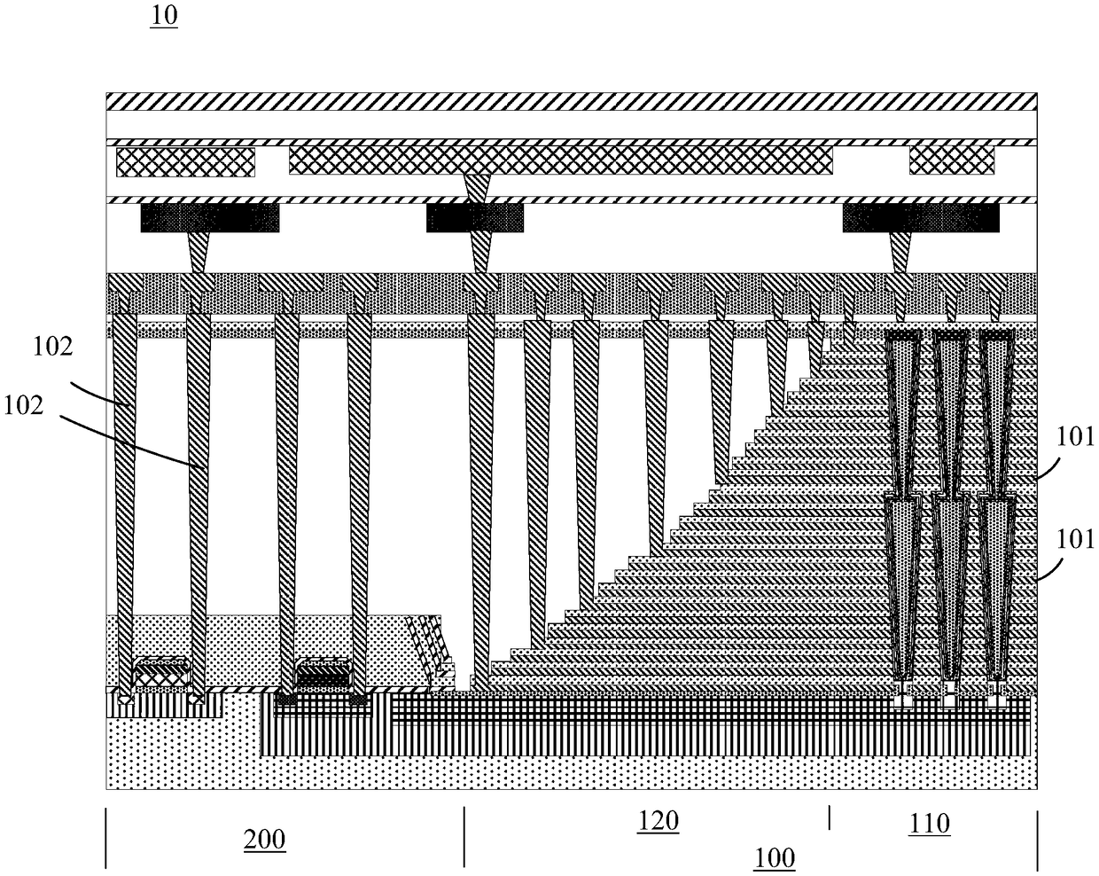
Pending Publication Date: 2018-11-16
YANGTZE MEMORY TECH CO LTD
View PDF11 Cites 4 Cited by
  • Summary
  • Abstract
  • Description
  • Claims
  • Application Information

AI Technical Summary

Problems solved by technology

The deviation of the contact portion from the corresponding stepped structure is also a common defect

Method used


Image

  • 3D memory word line connecting zone making method and 3D memory
  • 3D memory word line connecting zone making method and 3D memory
  • 3D memory word line connecting zone making method and 3D memory

Examples


Embodiment Construction

[0036] In order to make the above objects, features and advantages of the present invention more comprehensible, specific implementations of the present invention will be described in detail below in conjunction with the accompanying drawings.

[0037] In the following description, many specific details are set forth in order to fully understand the present invention, but the present invention can also be implemented in other ways than those described here, so the present invention is not limited by the specific embodiments disclosed below.

[0038] As indicated in this application and claims, the terms "a", "an", "an" and / or "the" do not refer to the singular and may include the plural unless the context clearly indicates an exception. Generally speaking, the terms "comprising" and "comprising" only suggest the inclusion of clearly identified steps and elements, and these steps and elements do not constitute an exclusive list, and the method or device may also contain other st...


PUM


Abstract

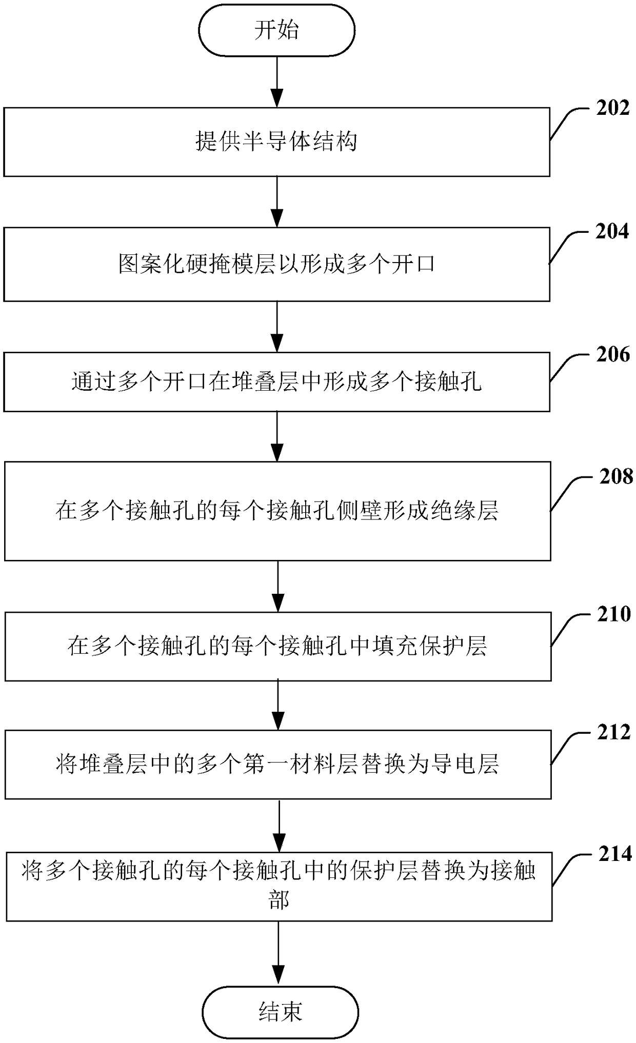
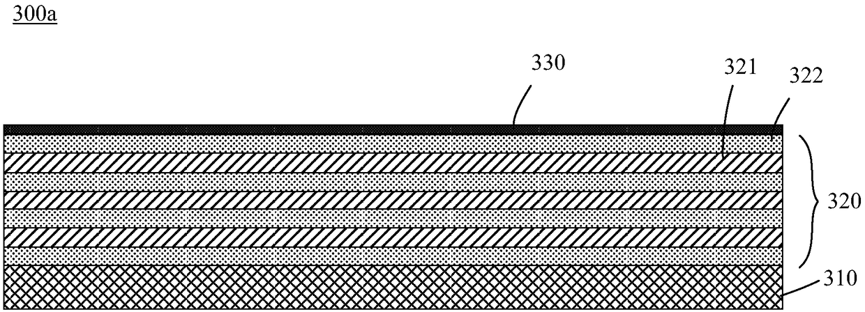
The invention relates to a 3D memory word line connecting zone making method and a 3D memory; the method comprises the following steps: providing a semiconductor structure that comprises a substrate,a stack layer covering the substrate and a hard mask layer covering the stack layer, wherein the stack layer comprises a plurality of first material layers and second material layers alternatively stacked; patterning the hard mask layer so as to form a plurality of openings the expose the stack layer; forming a plurality of contact holes in the stack layer via the plurality of openings, wherein each of the contact holes respectively reaches the first material layers at a self-configured depth; forming an insulation layer on the side wall of each of the contact holes; filling the insulation layer of the contact holes with a protection layer; replacing the first material layers in the stack layer with a conductive layer; forming a contact portion in each of the contact holes. The method canremove the etching defects of the word line connecting zone, and can solve the contact portion aligning problem.

Description

technical field [0001] The invention mainly relates to a semiconductor manufacturing method, in particular to a method for manufacturing a word line connection area of ​​a three-dimensional memory and the three-dimensional memory. Background technique [0002] In order to overcome the limitation of the two-dimensional memory, the industry has developed a memory having a three-dimensional (3D) structure, which improves integration density by three-dimensionally arranging memory cells on a substrate. [0003] In a three-dimensional memory such as 3D NAND flash memory, the memory array may include a core area and a stair step (SS) area. The stepped area is used for drawing out contact portions of the control gates in each layer of the memory array, and serves as a word line connection area. These control gates are used as word lines of the memory array to perform operations such as programming, erasing and writing, and reading. [0004] In the manufacturing process of 3D NAND...

Claims


Application Information

Patent Timeline
Patent Type & Authority Applications(China)
IPC IPC(8): H01L27/11578H01L27/11573H01L27/1157H10B43/20H10B43/35H10B43/40
CPCH10B43/40H10B43/20H10B43/35
Inventor 刘峻
Owner YANGTZE MEMORY TECH CO LTD
Learn More