Array substrate as well as manufacture method and display device thereof

A technology for array substrates and display devices, which is applied in semiconductor/solid-state device manufacturing, electrical components, electric solid-state devices, etc., and can solve problems such as easy breakage of connecting wires and low yield rate of display devices

Active Publication Date: 2018-11-27
BOE TECH GRP CO LTD
View PDF7 Cites 17 Cited by
  • Summary
  • Abstract
  • Description
  • Claims
  • Application Information

AI Technical Summary

Problems solved by technology

[0005] The present application provides an array substrate and its manufacturing method, and a display device, which can solve the problem that the existing connecting wires in the lead area are easily broken, resulting in a low yield rate of the display device

Method used


Image

  • Array substrate as well as manufacture method and display device thereof
  • Array substrate as well as manufacture method and display device thereof
  • Array substrate as well as manufacture method and display device thereof

Examples


Embodiment Construction

[0054] In order to make the object, technical solution and advantages of the present invention clearer, the implementation manner of the present invention will be further described in detail below in conjunction with the accompanying drawings.

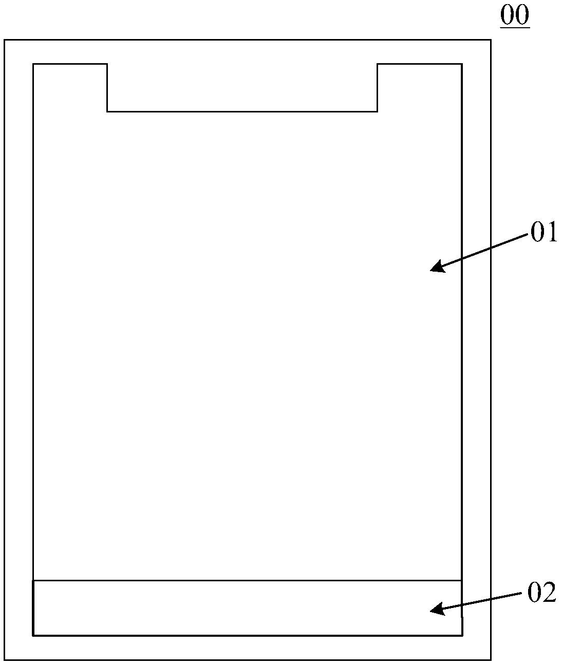
[0055] Please refer to figure 1 , figure 1 It is a schematic structural diagram of an array substrate provided in a display device in the related art. The array substrate 00 has a display area 01 and a lead area 02, and the display area 01 is provided with a plurality of signal lines ( figure 1 not shown in ), a plurality of connecting wires ( figure 1 Not shown in ), the connecting wire is used to connect the signal wire and the driver chip. For example, the multiple signal lines provided in the display area 01 may include multiple gate lines and multiple data lines, the driver chip may include a gate driver and a source driver, and the gate driver and multiple gate drivers may be realized through multiple connection lines. Line co...


PUM


Abstract

The invention discloses an array substrate as well as a manufacture method and display device thereof, belonging to the field of display technology. The array substrate comprises a substrate; the display area of the substrate is internally provided with a TFT (thin film transistor), the lead area of the substrate is internally provided with a through hole, and the through hole is internally provided with an organic filler; the lead area of the substrate is further internally provided with a connecting line, the connecting line is electrically connected with the TFT, and the materials for preparing the connecting line comprise a flexible conducting material. As the materials for preparing the connecting line comprise the flexible conducting material, the flexible conducing material has electrical conductivity and is difficult to fracture, therefore, when the lead area is bent, the probability that the connecting line is broken in the lead area is lowered, and the yield of display devices is effectively improved.

Description

technical field [0001] The present invention relates to the field of display technology, in particular to an array substrate, a manufacturing method thereof, and a display device. Background technique [0002] In order to improve the user's comfort in using the display device, the screen size of the display device is getting larger and larger, and the overall size of the display device is also getting larger with the increasing screen size. However, if the overall size of the display device exceeds a certain size, it will not only affect the user's use effect, but also affect the user's visual effect. Therefore, it is necessary to reduce the frame around the screen so that the overall size of the display device will not be too large. [0003] In the related art, a display device is usually provided with an array substrate. The array substrate has a display area and a lead area. The display area is provided with a plurality of signal lines. A plurality of connection lines, w...

Claims


Application Information

Patent Timeline
Patent Type & Authority Applications(China)
IPC IPC(8): H01L27/12H01L21/77
CPCH01L27/1244H01L27/1259H01L27/1218H01L27/1248H01L23/4985H10K59/131H10K71/00H10K77/111
Inventor 田雪雁刘政张帅
Owner BOE TECH GRP CO LTD
Why Eureka
Try Eureka