Active device array substrate and fabricating method thereof

Active Publication Date: 2011-09-22
AU OPTRONICS CORP
View PDF24 Cites 6 Cited by
  • Summary
  • Abstract
  • Description
  • Claims
  • Application Information

AI Technical Summary

Benefits of technology

[0006]The invention provides an active device array s

Problems solved by technology

As panel sizes of thin film transistor liquid crystal displays (TFT-LCD) become larger and larger, this enlargement is accompanied by resistor capacitor (RC) delay effects caused by resistance values of metal wires wh

Method used


Image

  • Active device array substrate and fabricating method thereof
  • Active device array substrate and fabricating method thereof
  • Active device array substrate and fabricating method thereof

Examples


Embodiment Construction

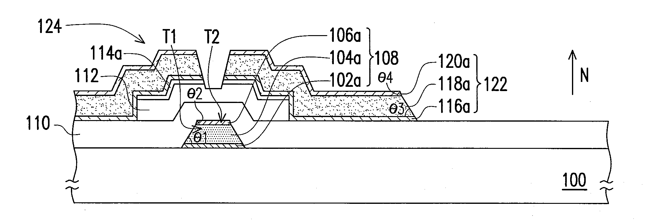
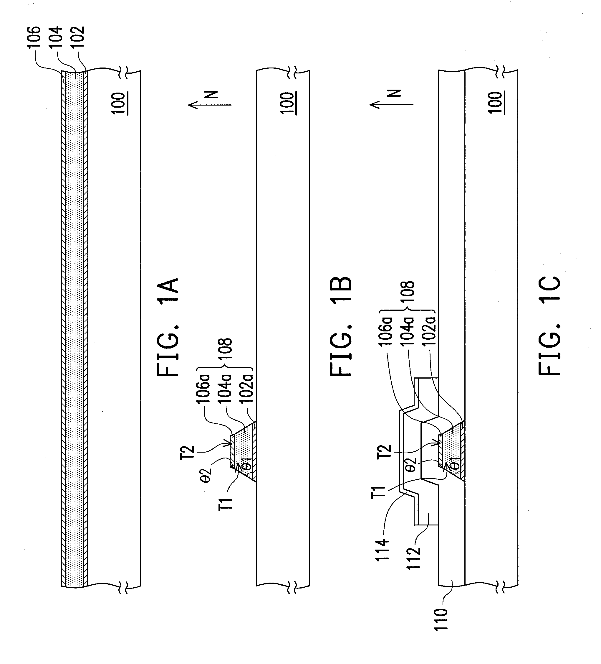
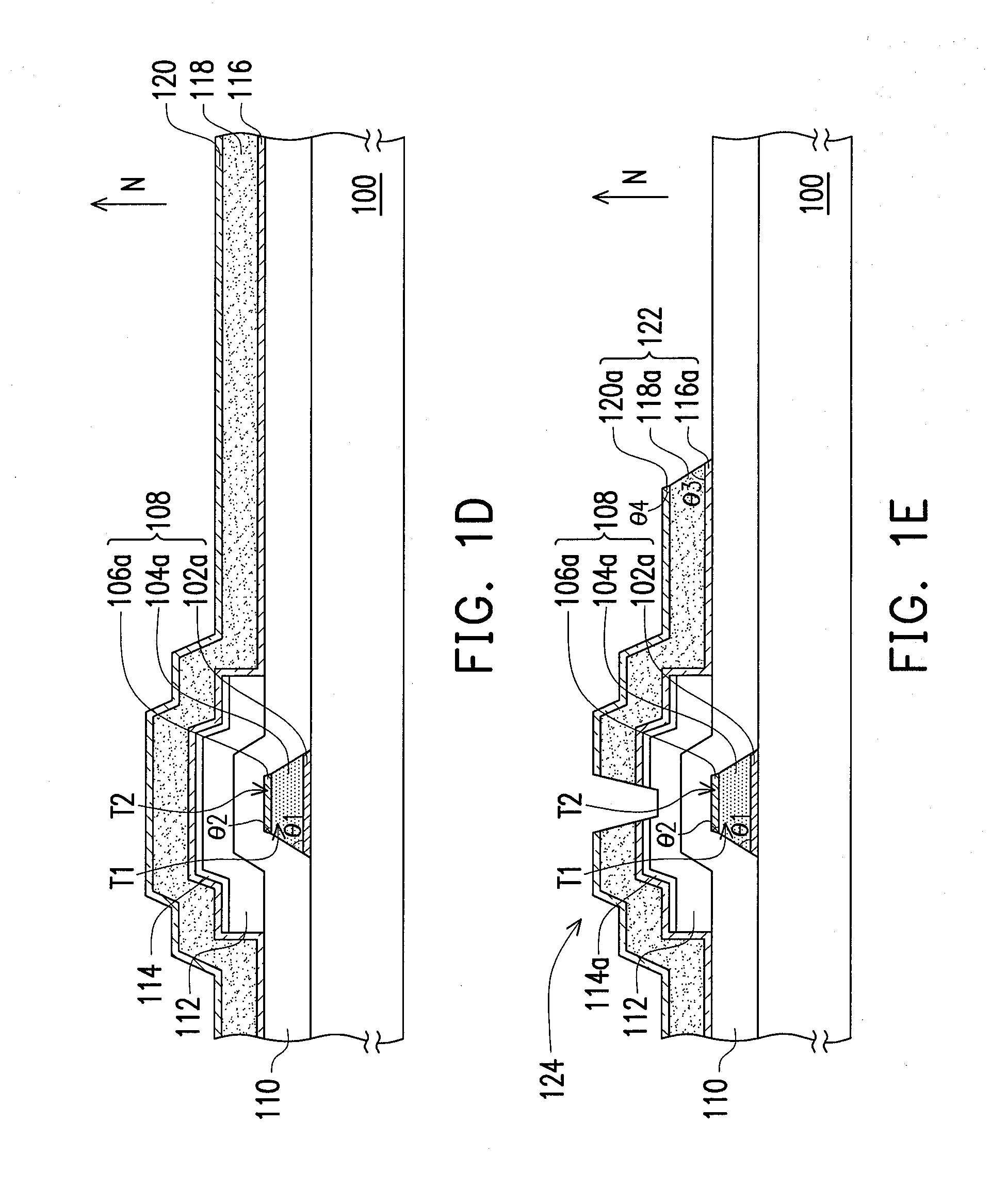
[0029]FIGS. 1A to 1G are schematic cross-sectional views showing a fabrication process of an active device array substrate according to an embodiment of the invention. FIG. 2 is a schematic cross-sectional view along another direction of a patterned conductive layer 122 in FIG. 1E, wherein the cross-section direction of FIG. 2 is perpendicular to the cross-section direction of FIG. 1E.

[0030]First, please refer to FIG. 1A. A substrate 100 is provided. The material of the substrate 100 is a transparent material, a non-transparent material, a flexible material, or any combination of the above.

[0031]Next, a barrier layer 102 is optionally / selectively formed on the substrate 100. The material of the barrier layer 102 is at least one selected from the group consisting of molybdenum, a molybdenum alloy, titanium, a titanium alloy, an aluminum alloy, and a copper alloy. The method of forming the barrier layer 102 is, for example, a physical vapor deposition method.

[0032]Next, a copper layer...


PUM

PropertyMeasurementUnit
Angleaaaaaaaaaa
Angleaaaaaaaaaa
Angleaaaaaaaaaa

Abstract

An active device array substrate has at least one patterned conductive layer. The patterned conductive layer includes a copper layer. A cross-section of the copper layer which is parallel to a normal line direction of the copper layer includes a first trapezoid and a second trapezoid stacked on the first trapezoid. A base angle of the first trapezoid and a base angle of the second trapezoid are acute angles, and a difference between the base angle of the first trapezoid and the base angle of the second trapezoid is from about 5° to about 30°.

Description

CROSS-REFERENCE TO RELATED APPLICATION[0001]This application claims the priority benefit of Taiwan application serial no. 99108356, filed on Mar. 22, 2010. The entirety of the above-mentioned patent application is hereby incorporated by reference herein and made a part of this specification.BACKGROUND OF THE INVENTION[0002]1. Field of the Invention[0003]The invention is related to an active device array substrate, and in particular to an active device array substrate which has a copper conductive layer.[0004]2. Description of Related Art[0005]As panel sizes of thin film transistor liquid crystal displays (TFT-LCD) become larger and larger, this enlargement is accompanied by resistor capacitor (RC) delay effects caused by resistance values of metal wires which are not low enough. Signals are hence distorted during transmission, thereby affecting the display quality of the panels. By using a single layer of copper which has low resistance as a metal wire, RC delay effects are effectiv...

Claims


Application Information

Patent Timeline
IPC IPC(8): H05K7/00B05D5/12C23C14/34H05K1/09
CPCC23C14/165C23C14/3492H01L27/124H01L29/4908H01L29/458
Inventor CHEN, PO-LINLIN, CHIH-YUANLIN, YU-MINLIN, CHUN-NAN
Owner AU OPTRONICS CORP
Why Eureka
Try Eureka