

Y-gate transistor device and manufacturing method thereof
A device manufacturing method and transistor technology, applied in semiconductor/solid-state device manufacturing, semiconductor devices, electrical components, etc., can solve the problems of Y-gate semiconductor manufacturing steps, etc., to increase cross-sectional area, reduce cost, and improve efficiency Effect
- Summary
- Abstract
- Description
- Claims
- Application Information
AI Technical Summary
Problems solved by technology
Method used
Image

Examples
Embodiment Construction
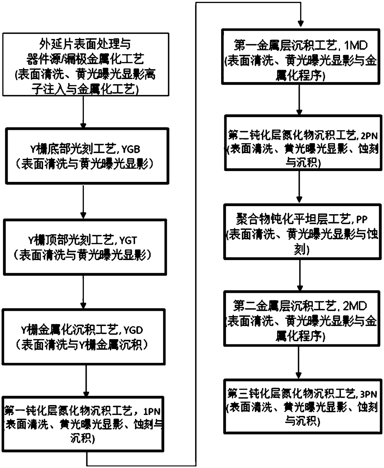
[0035] In order to explain in detail the technical content, structural features, achieved goals and effects of the technical solution, the following will be described in detail in conjunction with specific embodiments and accompanying drawings.
[0036] First, explain the English nouns that may appear:
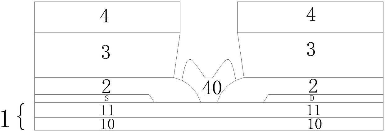
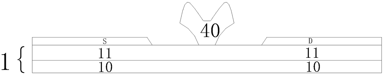
[0037] 1. YGB: Y-Gate Bottom, Y-gate bottom photolithography process;
[0038] 2. YGT: Y-Gate Top, Y-gate top photolithography process;
[0039] 3.YGD: Y-Gate Deposition, Y gate metallization deposition process;
[0040] 4.1PN: 1st Passivation Nitride, the first passivation layer nitride deposition process;
[0041] 5.1MD: 1st Metal Deposition, the first metal layer deposition process;
[0042] 6.2PN: 2nd Passivation Nitride, the second passivation layer nitride deposition process;
[0043] 7.PP: Polyimide Passivation, polymer passivation flat layer process;
[0044] 8.2MD: 2nd Metal Deposition, the second metal layer deposition process;
[0045] 9.3PN: 3rd Passivation N...
PUM
 Abstract
Description
Claims
Application Information