

Semiconductor device and preparation method thereof
A semiconductor and device technology, applied in the field of semiconductor devices and their preparation, can solve problems such as reducing gate resistance, affecting device frequency characteristics, increasing gate parasitic capacitance, etc., to reduce gate resistance, increase cross-sectional area, and reduce parasitic The effect of capacitance
- Summary
- Abstract
- Description
- Claims
- Application Information
AI Technical Summary
Problems solved by technology
Method used
Image

Examples
preparation example Construction
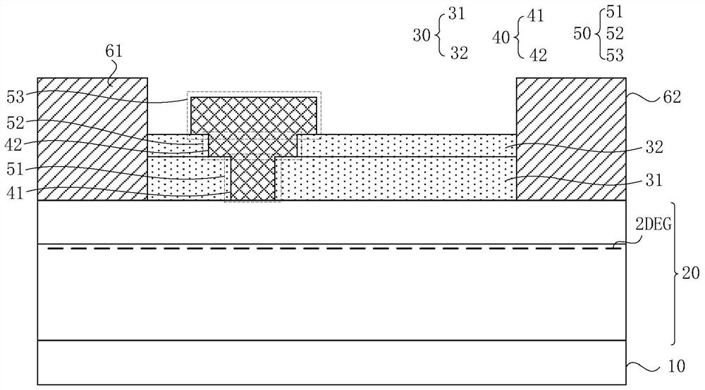
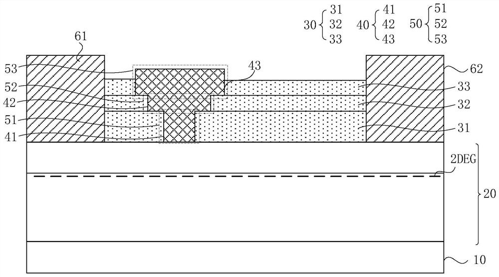
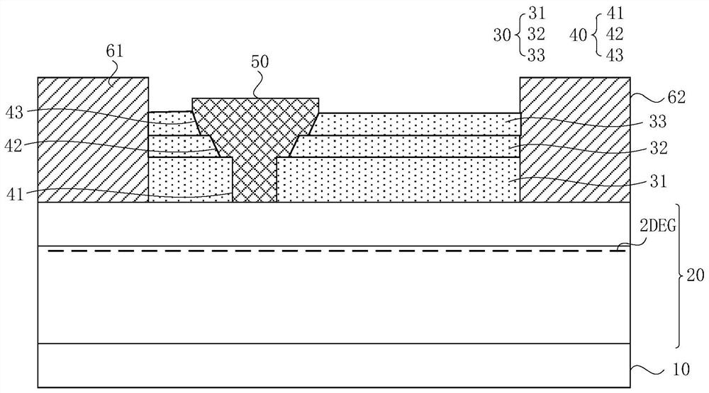
[0088] Based on the same inventive concept, an embodiment of the present invention also provides a method for manufacturing a semiconductor device, which is used to prepare the semiconductor device provided in any one of the above embodiments. Figure 8 is a schematic flow chart of a method for manufacturing a semiconductor device provided by an embodiment of the present invention, Figure 9 With Figure 8 The schematic diagram of the preparation process of the semiconductor device corresponding to the preparation method shown, with figure 1 The fabrication process of the shown semiconductor device is illustrated as an example. see Figure 8 with Figure 9 , the preparation method may specifically include the following steps:
[0089] S11. Providing a substrate.
[0090] S12, preparing multiple semiconductor layers on one side of the substrate.
[0091] For the structures of the substrate and the multi-layer semiconductor layers, please refer to the description of the se...
PUM
 Abstract
Description
Claims
Application Information