Manufacturing method of semiconductor device

A manufacturing method and semiconductor technology, applied in the direction of semiconductor devices, electrical solid devices, electrical components, etc., can solve problems affecting device performance, abnormal contour and depth, etc., to ensure contour and depth, ensure performance, and avoid sparse/dense load effect of effect

Active Publication Date: 2020-07-28
SEMICON MFG INT TIANJIN +1
View PDF4 Cites 0 Cited by
  • Summary
  • Abstract
  • Description
  • Claims
  • Application Information

AI Technical Summary

Problems solved by technology

It has been found in practice that when the gates of the dense region and the sparse region are formed in the same etching process, there is an etching difference (I / D loading, or known as sparse / dense loading effect), affected by the I / D loading, the gates at the edge of the dense area tend to have abnormal contours and depths, and the abnormal edge gates will have an abnormality in the middle of the dense area. Both the gate and the gate of the sparse region are adversely affected, which in turn affects the performance of the device

Method used


Image

  • Manufacturing method of semiconductor device
  • Manufacturing method of semiconductor device
  • Manufacturing method of semiconductor device

Examples


Embodiment Construction

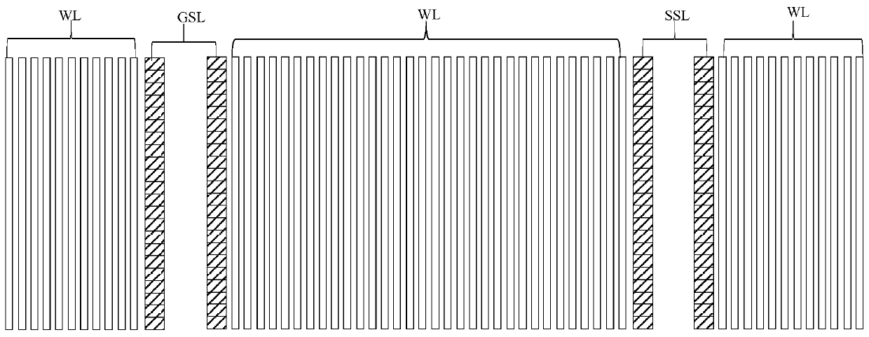
[0037] Such as figure 1 As shown, the NAND flash memory device may include: a plurality of parallel active regions (ACT, not shown) in a semiconductor substrate separated by a device isolation layer, a ground select gate line (GSL), a string select gate line (SSL) and a plurality of word lines (WL) arranged between adjacent GSLs and SSLs, the GSLs are formed by connecting the gates of the ground selection transistors together, and the sources or drains of these ground selection transistors are connected to the source lines ( SL), SSL is formed by connecting the gates of string selection transistors together, and the source or drain of these string selection transistors is connected to the bit line (BL), and WL is connected by the control gates of the memory cells on the same active area. Formed together, SSL, GSL, WL are arranged in parallel and cross the active region (ACT), and a corresponding charge storage structure can be provided between each WL and each active region (A...


PUM


Abstract

The invention provides a method for manufacturing a semiconductor device. After depositing a side wall material layer on the surface of the first patterned layer, firstly form a second patterned layer corresponding to the first grid on the side wall material layer, and then use The second patterned layer is a mask, and the side wall material layer is etched to form a third patterned layer with the first gate pattern and the second gate pattern, because the third patterned layer has no serious sparse / dense load effect, so using the third patterned layer as a mask to etch the gate layer to form the first gate and the second gate have no etching difference, avoiding the sparse / dense loading effect of the gate and avoiding abnormalities The appearance of the edge second gate further ensures the performance of the manufactured semiconductor device.

Description

technical field [0001] The invention relates to the technical field of integrated circuit manufacturing, in particular to a method for manufacturing a semiconductor device. Background technique [0002] At present, with the rapid development of ultra-large-scale integrated circuits, the integration of chips is getting higher and higher, and the circuit design size is getting smaller and smaller. The various effects caused by the high density and small size of devices have an increasing impact on the semiconductor manufacturing results. It is outstanding that, especially in the process below the 28nm technology node, the change of the critical dimension (CD, Critical Dimension) of the circuit has more and more influence on the performance of the device. As we all know, since the gate usually has the smallest physical size in the semiconductor manufacturing process, and the width of the gate is usually the most important critical dimension on the wafer, the fabrication of the ...

Claims


Application Information

Patent Timeline
Patent Type & Authority Patents(China)
IPC IPC(8): H01L27/11517
CPCH10B41/00
Inventor 王彦陈卓凡
Owner SEMICON MFG INT TIANJIN
Why Eureka
Try Eureka