1D1R memory with single stacking structure, and preparation method thereof

A memory and heterogeneous structure technology, applied in the field of information storage, can solve the problems of increasing the complexity of the manufacturing process and high cost, and achieve the effects of increasing 3D integration density, suppressing cross-generation problems, and simplifying the manufacturing process

Inactive Publication Date: 2018-12-07
INST OF PHYSICS - CHINESE ACAD OF SCI
View PDF3 Cites 0 Cited by
  • Summary
  • Abstract
  • Description
  • Claims
  • Application Information

AI Technical Summary

Problems solved by technology

Among them, the traditional 1D1R device usually uses an RRAM and a diode in series, which will undoubtedly increase the complexity of the manufacturing process and make the cost higher

Method used


Image

  • 1D1R memory with single stacking structure, and preparation method thereof
  • 1D1R memory with single stacking structure, and preparation method thereof
  • 1D1R memory with single stacking structure, and preparation method thereof

Examples


no. 1 example

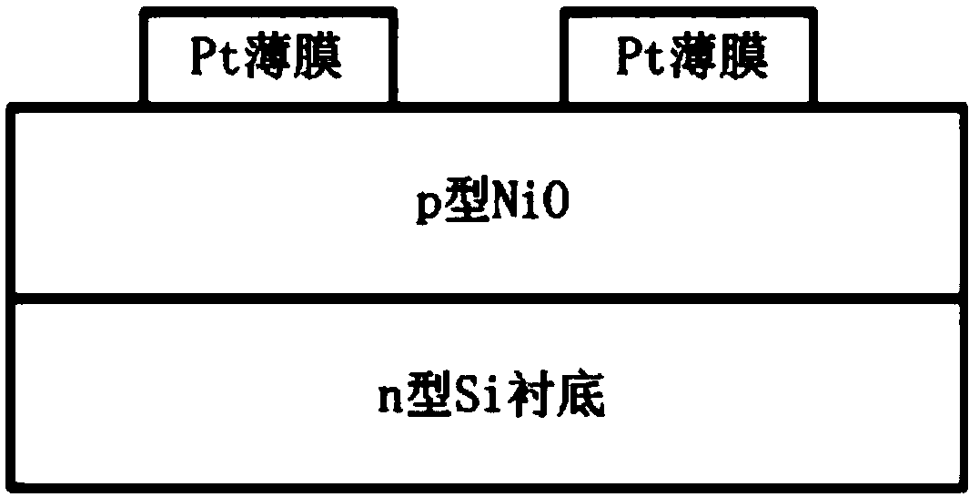
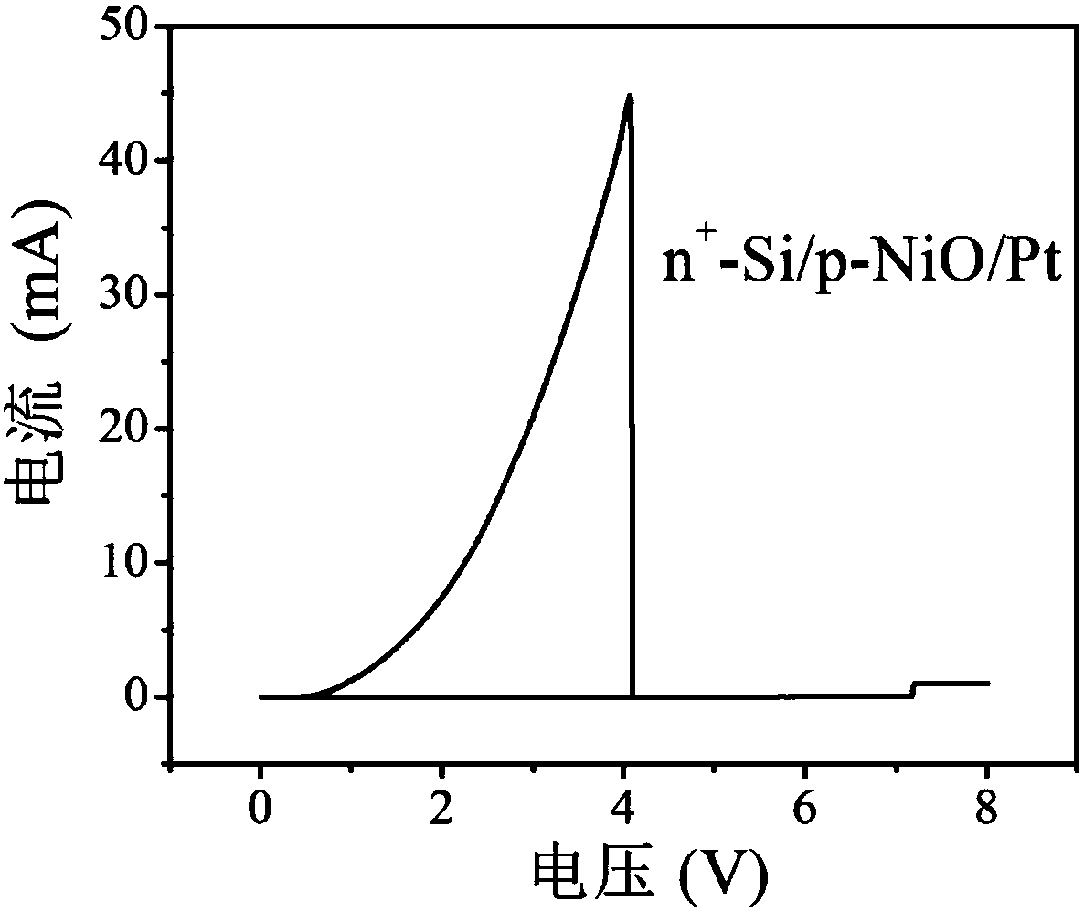
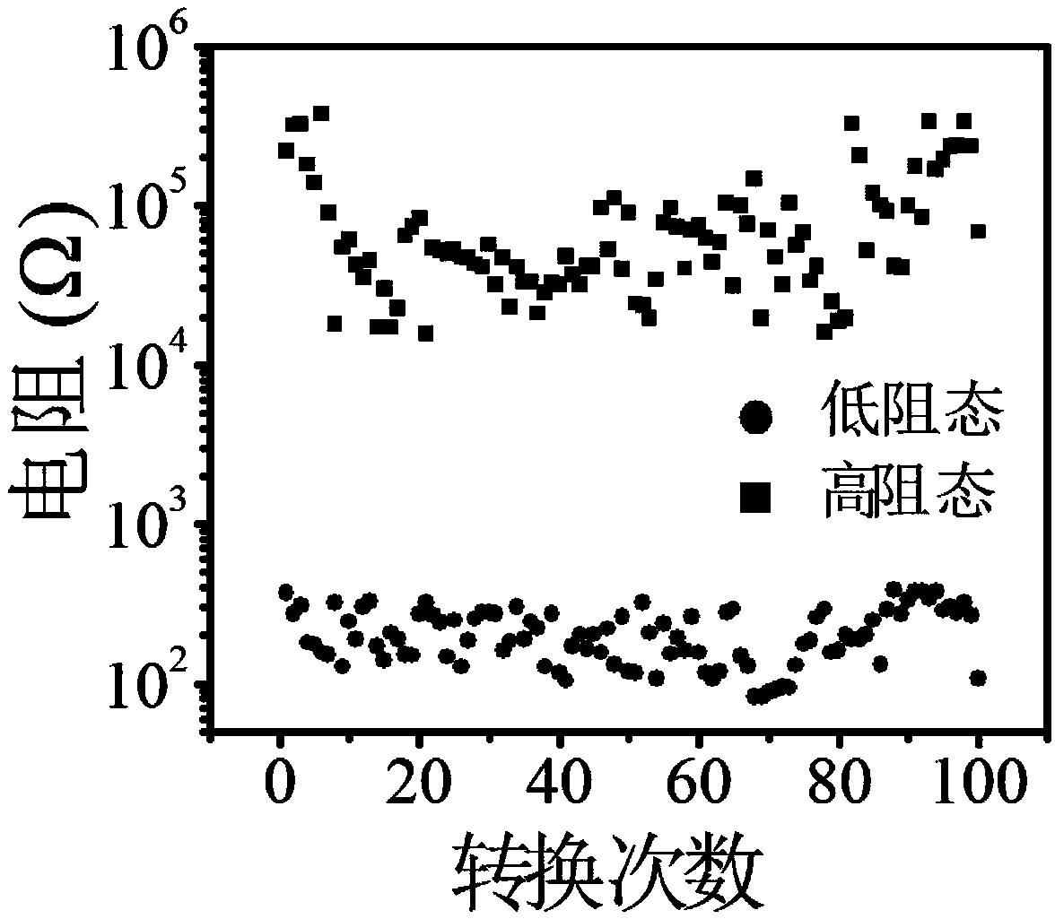
[0028] This embodiment provides a 1D1R memory with a single stack structure, the structure of which is as follows figure 1 As shown, including n-type Si substrate, p-type NiO film on n-type Si substrate, and Pt film on p-type NiO film, wherein the resistivity of the n-type Si substrate is about 0.01-0.05 Ω*cm, the resistivity of the p-type NiO film is about 10 4 -10 5 Ω*cm, thickness about 60nm, the thickness of the Pt thin film is about 150nm, and the shape is a circular array with a diameter of 400μm.

[0029] In this embodiment, the n-type Si substrate and the p-type NiO film form a pn heterostructure (1D), so that the formed device has rectification characteristics. At the same time, the n-type Si substrate has low resistivity and high conductivity It can be used as the bottom electrode, and the p-type NiO film can be used as a resistive layer (1R) due to its high resistivity and low conductivity to realize the high-low resistance switching of the device; the Pt film is ...

no. 2 example

[0036] This embodiment provides another 1D1R memory with a single stack structure, its structure is as follows Figure 5 As shown, including p-type Si substrate, n-type ZnO film on p-type Si substrate, and Al film on n-type ZnO film, wherein the resistivity of the p-type Si substrate is about 0.01-0.05 Ω*cm, the resistivity of the n-type ZnO film is about 10 4 -10 5 Ω*cm and a thickness of about 100nm, the thickness of the Al thin film is about 80nm.

[0037] In this embodiment, the p-type Si substrate and the n-type ZnO film form a pn heterostructure (1D), so that the formed device has rectification characteristics. At the same time, the p-type Si substrate has low resistivity and high conductivity Can be used as a bottom electrode, n-type ZnO film can be used as a resistive layer (1R) due to its high resistivity and low conductivity to realize high-low resistance switching of devices; Al film is used as a metal film top electrode, and its work function is the same as that ...


PUM

PropertyMeasurementUnit
Thicknessaaaaaaaaaa
Thicknessaaaaaaaaaa
Thicknessaaaaaaaaaa

Abstract

The present invention provides a 1D1R memory. The 1D1R memory includes: an Si substrate layer, a metal oxide layer over the Si substrate layer, and a metal electrode layer over the metal oxide layer,wherein the Si substrate layer and the metal oxide layer constitute a pn heterostructure; the Si substrate layer has a resistivity of 0.01 to 0.05 Omega*cm; the metal oxide layer has a resistivity of10<4> to 10<5> Omega*cm; and the work function of the metal electrode layer matches the Fermi level of the metal oxide layer. The 1D1R memory has a single stacking structure, has a simple preparationprocess, and has a high longitudinal 3D integration density.

Description

technical field [0001] The invention belongs to the field of information storage, in particular to a 1D1R memory with a single stack structure and a preparation method thereof. Background technique [0002] With the progress of society, the traditional non-volatile memory can no longer meet people's requirements for high speed, high density, and low energy consumption. Therefore, it is urgent to develop a new generation of non-volatile memory. Resistive random access memory (RRAM) stands out among many non-volatile memories due to its simple structure, high storage density, high switching speed, low energy consumption and long retention time. [0003] In order to realize the large-area application of RRAM devices, the key is to realize the integration of a large number of RRAM devices, but such integrated circuit devices arranged vertically and horizontally will encounter the problem of crosstalk. To overcome the crosstalk problem, some device structures have been proposed,...

Claims


Application Information

Patent Timeline
IPC IPC(8): H01L27/24H01L45/00
CPCH10B63/20H10N70/257H10N70/24H10N70/011
Inventor 张磊白雪冬许智
Owner INST OF PHYSICS - CHINESE ACAD OF SCI
Why Eureka
Try Eureka